You are currently viewing SemiWiki as a guest which gives you limited access to the site. To view blog comments and experience other SemiWiki features you must be a registered member. Registration is fast, simple, and absolutely free so please,
join our community today!
Walking across a carpet can generate up to 35,000 volts of static charge, which is tens of thousands of times higher than the operating voltages of most integrated circuits. When charge build up from static electricity is exposed to the pins of an IC, the electrostatic discharge (ESD) protection network on the chip is intended to… Read More
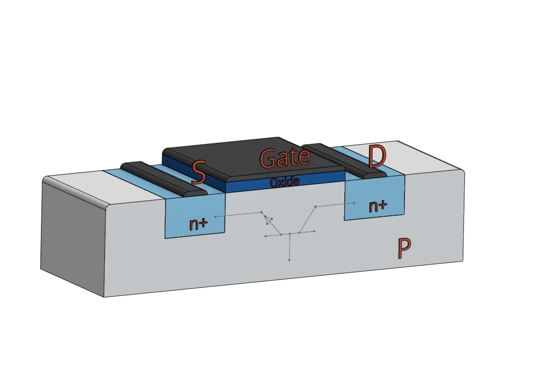
Lurking inside of every Mosfet is a parasitic bipolar junction transistor (BJT). Of course, in normal circuit operation the BJT does not play a role in the device operation. Accordingly, SPICE models for Mosfets do not behave well when the BJT is triggered. However, these models work just fine for most purposes. The one important… Read More
Terms like avalanche breakdown and impact ionization sound like they come from the world of science fiction. They do indeed come from a high stakes world, but one that plays out over and over again here and now, on a microscopic scale in semiconductor devices – namely as part of electrostatic discharge (ESD) protection. Semiconductor… Read More