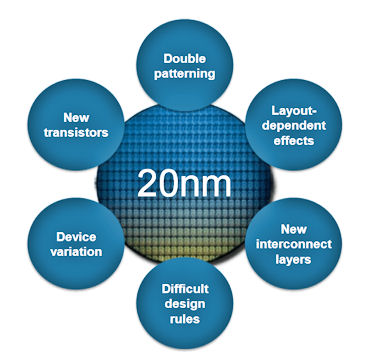
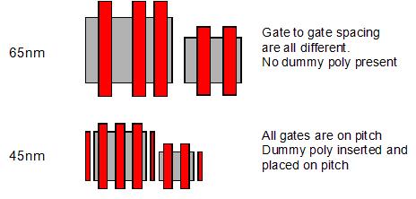
Standard cell library developers are faced with a daunting task when it is time to create a library for a new process node. Porting an existing library can be a big help, but even then, manual modifications to 800 or more cells is still required. Each of those cells has many geometric elements are that affected by new design rules. All… Read More
Tag: process migration
Whitepaper : The True Costs of Process Node Migration
Mentor, A Siemens Business, just released a new white paper entitled, “The True Costs of Process Node Migration” written by John Ferguson. This is a good quick read that highlights some of the key areas that are often over looked when contemplating a shift of process nodes for your next design.
When considering a shift to a more advanced… Read More
Sagantec’s nmigrate adopted and deployed for 14nm technology
Major semiconductor company successfully migrated 28nm libraries to 14nm FinFET
Santa Clara, California – May 29, 2013 – Sagantec announced that its nmigrate tool was adopted by a major semiconductor company for the development of standard cell libraries at 14nm and 16nm FinFET technologies.
This customer already… Read More
Sagantec Update: More EDA Consolidation!
Adding sophisticated 2D dynamic compaction technology to address 20nm and 14nm challenges. Santa Clara, California – May 3 ,2012 – Sagantec today announced that it has acquired Dutch startup NP-Komplete Technologies BV (Eindhoven, The Netherlands) for its physical design compaction and migration solutions based on a sophisticated… Read More
Sagantec 2 Migrate iPad2s @ #48DAC
Sagantec is the leading EDA provider of process migration solutions for custom IC design. Sagantec’s EDA solutions enable IC designers to leverage their investment in existing physical design IP and accomplish dramatic time and effort savings in the implementation of custom, analog, mixed-signal and memory circuits… Read More
65nm to 45nm SerDes IP Migration Success Story
The problem:To move a single lane variable data rate SerDes (serializer-deserializer) from a 65nm process to a 45nm process, achieving a maximum performance of up to 10.3 Gbps. This is a large piece of complex mixed-signal IP with handcrafted analog circuits. Circuit performance and robustness are critical and must be maintained… Read More
Adjusting Custom IP to Process Changes
A High-Definition Multimedia Interface (HDMI) IP core was being implemented in an advanced process technology. This fairly large and complex analog mixed-signal (AMS) IP comprising over 130K devices was close to being finalized and shipped to the customer. But many design rules at the foundry were unexpectedly changed from… Read More
Semiconductor Wafer Allocation and Design Migration
In the name of blogging and increased transparency lets talk about wafer allocation, because it’s coming, believe it. There is already a significant delta between wafer demand and manufacture due to record low inventory levels and the exploding semiconductor demand in China. Both TSMC and UMC posted good July sales numbers: … Read More


