You are currently viewing SemiWiki as a guest which gives you limited access to the site. To view blog comments and experience other SemiWiki features you must be a registered member. Registration is fast, simple, and absolutely free so please,
join our community today!
Daniel is joined by David Liberman, a Los Angeles-based futurist, serial entrepreneur, investor, and former Director of Products at Snap, as well as the co-creator of the Gonka protocol. Gonka is a decentralized protocol that connects people who need computing power for AI with operators who provide GPU hardware. Its goal is … Read More
In this webinar, Google Cloud and NetApp explore how semiconductor companies can address the growing infrastructure demands of modern Electronic Design Automation (EDA) workflows. As process technologies continue to advance and chip designs become increasingly complex, engineering teams require scalable, high-performance… Read More
On July 9, 2025, a DACtv session featured a Google product manager discussing the strategic importance of electronic design automation (EDA) and how Google Cloud is optimizing it for the semiconductor industry, as presented in the YouTube video. The talk highlighted Google Cloud’s role in addressing the escalating complexity… Read More
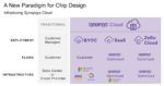
There’s been a lot of discussion and hype regarding use of the cloud for chip design for quite a while, more than ten years I would say. I spoke with Synopsys to better understand their recent Synopsys Cloud announcement to determine if it is different. Briefly, it is different, and here is why:
If you’re trying to design a complex SoC,… Read More
We all know that design complexity is increasing at a fast pace. There’s always more analysis to run on larger and larger volumes of data. During tapeout, these demands can grow by an order of magnitude. Successful design projects need to add huge amounts of CPU, memory and storage for short bursts of time during tapeout to meet their… Read More