You are currently viewing SemiWiki as a guest which gives you limited access to the site. To view blog comments and experience other SemiWiki features you must be a registered member. Registration is fast, simple, and absolutely free so please,
join our community today!
WP_Term Object
(
    [term_id] => 158
    [name] => Foundries
    [slug] => semiconductor-manufacturers
    [term_group] => 0
    [term_taxonomy_id] => 158
    [taxonomy] => category
    [description] =>
    [parent] => 0
    [count] => 1364
    [filter] => raw
    [cat_ID] => 158
    [category_count] => 1364
    [category_description] =>
    [cat_name] => Foundries
    [category_nicename] => semiconductor-manufacturers
    [category_parent] => 0
    [is_post] =>
)
When I do a root cause analysis of Intel’s problem it is very simple. If Intel wants to continue to be a leading-edge semiconductor manufacturer, they need to fill their fabs, all of their fabs. Clearly several things need to happen in order to do that but the one that most interests me is on the foundry side.
I think we can all agree that… Read More
One of the most enduring threads in the SemiWiki forum is What would you do if you are the Intel CEO? There are currently 128 responses and more than 45,000 views. It was originally posted March 13th, 2015, after Brain Krzanich was given the CEO position. A different time for sure but an interesting read and the responses keep on coming.… Read More
IEDM was buzzing with many presentations about the newest gate-all-around transistor. Both Intel and TSMC announced processes based on nanosheet technology. This significant process innovation allows the fabrication of silicon RibbonFET CMOS devices, which promise to open a new era of transistor scaling, keeping Moore’s… Read More
There was a lot of discussion at IEDM about the coming shift to gate-all-around (GAA) transistor structures. This new device brings many benefits to continue device scaling, both at the monolithic device level as well as for multi-die design. The path to GAA is not simple, there are new material, process and design considerations… Read More
A response to Daniel Nenni’s “What’s Wrong with Intel?” article, which invited alternative views.
At the risk of calling down the forecast universal opprobrium, I’m going to disagree with Dan’s take on the centrality of Intel.
I don’t agree that Intel is too big/important to fail or that the US can’t succeed in semiconductors without… Read More
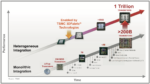
IEDM turned 70 last week. This was cause for much celebration in the form of special events. One such event was a special invited paper on Tuesday afternoon from Intel’s Tahir Ghani, or Mr. Transistor as he is known. Tahir has been driving innovation at Intel for a very long time. He is an eyewitness to the incredible impact of the Moore’s… Read More
The main program for the 70th IEDM opened on Monday morning in San Francisco with an excellent keynote from Dr. Yuh-Jier Mii, Executive Vice President and Co-Chief Operating Officer at TSMC. Dr. Mii joined TSMC in 1994. Since then, he has contributed to the development and manufacturing of advanced CMOS technologies in both fab
…
Read More
One of the most popular topics on the SemiWiki forum is Intel, which I understand. Many of us grew up with Intel, some of us have worked there, and I can say that the vast majority of us want Intel to succeed. The latest Intel PR debacle is the abrupt departure of CEO Pat Gelsinger. To me this confirms the answer to the question, “What is … Read More
Dan is joined by Dr. Tahir Ghani, Intel senior fellow and director of process pathfinding in Intel’s Technology Research Group. Tahir has a 30-year career at Intel working on many innovations, including strained silicon, high-K metal gate devices, FinFETs, RibbonFETs, and backside power delivery (BSPD), among others. He has… Read More
WIth packaging being one of the top sources of traffic on SemiWiki, I am expecting a big crowd at this event. A semiconductor substrate is a foundational material used in the fabrication of semiconductor devices. Substrates are a critical part of the manufacturing process and directly affect the performance, reliability, and… Read More


Musk’s Orbital Compute Vision: TERAFAB and the End of the Terrestrial Data Center