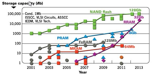
 A lot has been happening in the ReRAM world over the past couple of months. At the ISSCC Conference in February Toshiba/SanDisk presented a paper describing a 32Gbit ReRAM chip. The chip is a bilayer of two crosspoint arrays fabricated one on top of the other sharing the set of wires (designated as bit lines by the authors) fabricated between the arrays. Each cell at the intersection of the bit and word lines comprises of a metal oxide layer and diode access device. Thus the stack of the bilayer (in order of fabrication) is Word Line-Diode/MeOx-Shared Bit Line-Diode/MeOx-Word Line. The bilayer is fabricated with a 24nm technology. The arrays are fabricated in the BEOL over circuitry in the under lying Si. The arrays are organized in ‘Bays’ which each comprise of 32 by 4 (128) mini bilayer cross point arrays which in turn comprise of 2k Bit Lines and 4k Word Lines to give 8 million cells per mini array per layer. The chip is currently one bit per cell although the authors believe MLC (and more layers) are possible. This is an impressive development and shows a huge commitment in terms of design and processing by the two companies involved. This represents a huge advance for ReRAM technology. After all the chip has a 500x greater capacity than the previous ReRAM ‘record’ and incorporates multiple memory layers, another first at this density. Nonetheless, I expect commercialization is a way off. But a few weeks later, on the other side of the Globe and admittedly a far lower density, an ReRAM containing product was announced…..
 At the 2013 Embedded World Exhibition in Nuremberg, Panasonic announced their ReRAM ontaining MCU. The product is described as “8-bit low-power-consumption microcomputer: Delivers both smaller area and small ROM code size as 8-bit microcomputer and high performance as 16-bit microcomputer based on 16-bit microcomputer core with alterable (3 or 4) stage pipeline. It also delivers lower power consumption of the system by intermittent operation.” It contains 128kB (program) + 8kB (data) of ReRAM which permits “No more need for sector erase, erase and rewrite memory at byte level”. Interestingly the data area ReRAM is quoted as having a 100x higher endurance than the program area ReRAM. The cell is BEOL with a TaOx layer sandwiched between unidentified top and bottom electrode. The main selling point is lower power consumption due to a peak current reduction due to ReRAM and a current pulse width reduction due to a faster CPU and reduced leakage. The net is a 50% reduction in the average current.
The spring meeting season is in full swing with the 2013 Symposia on VLSI Technology and Circuits in Kyoto coming up in June. The Fifth IEEE International Memory Workshop (IMW 2013) takes place in Monterey at the end of May and 2013 VLSI-TSA in Hsinchu, takes place towards the end of April. All have multiple sessions devoted to emerging memories including ReRAM and CBRAM. Last but not least, the Adesto Technologies Workshop on Non-volatile Memory Solutions takes place on 4/25 in San Jose, CA.  For more details and links check out ReRAM-Forum.com. You will also find a number of recent topics of discussions including a description of how Si Valley start-up Intermolecular is impacting ReRAM development of some key players in the memory business….
lang: en_US
Share this post via:


Musk’s Orbital Compute Vision: TERAFAB and the End of the Terrestrial Data Center