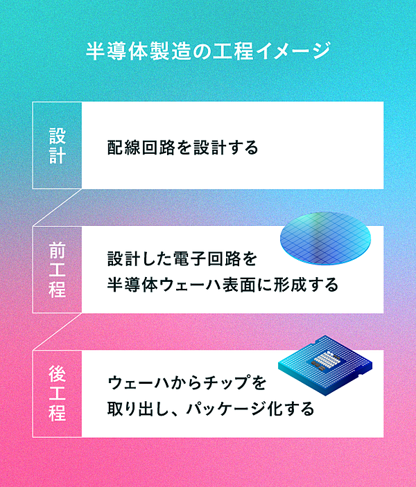
For the past few decades, semiconductor evolution has revolved around miniaturization in the "front-end" of manufacturing. However, with the rise of generative AI, semiconductors are now required to have unprecedented computing power, and attention is now turning to technological innovation in the "back-end"—a field that has traditionally been relatively neglected.
TSMC, a Taiwanese semiconductor contract manufacturer, has been strengthening its research and development in back-end manufacturing over the past decade.
It may not be widely known that TSMC has established a research and development center for advanced packaging technology in Tsukuba, Japan. However, the foundation for co-creation with Japanese companies has already been laid.
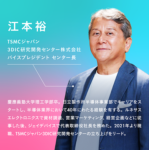
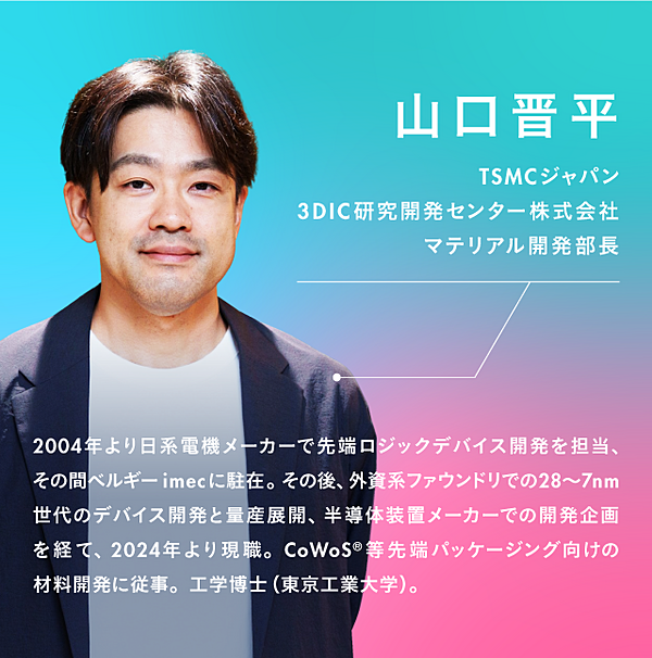
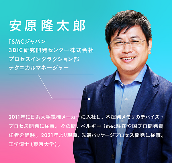
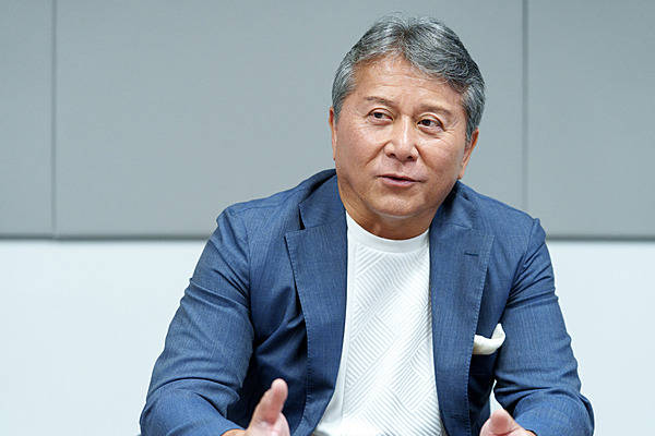
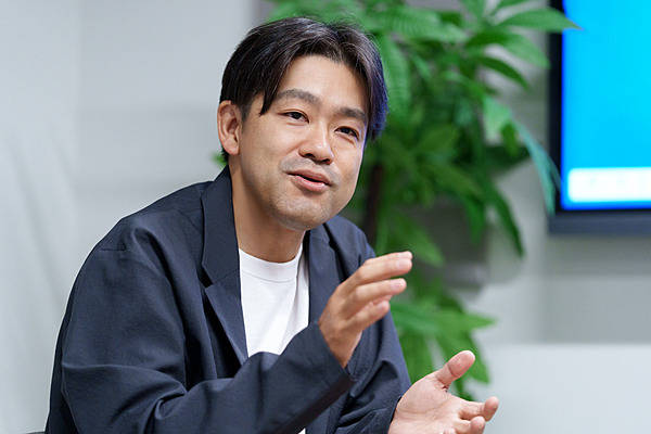
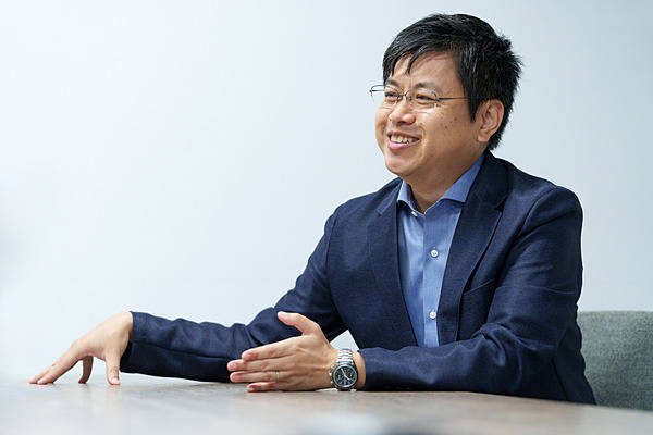
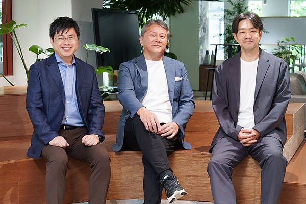
Why is TSMC based in Japan and promoting collaboration with Japanese companies? We spoke with Yutaka Emoto, director of the TSMC Japan 3DIC Research and Development Center (hereinafter referred to as the 3DIC Research and Development Center), the center's base; Shinpei Yamaguchi , who leads materials development on-site; and Ryutaro Yasuhara , who is responsible for process development .
Emoto : Yes, that's right. I am the director of the research and development center for this "post-processing" but I actually don't like the term "post-processing."
Traditionally, downstream processes in manufacturing have been considered to be little more than "assembling finished parts," and have been considered less technically difficult than upstream processes.
However, the cutting edge of semiconductor manufacturing today is something completely different from "simple assembly work." It has evolved into the field of "advanced packaging," which requires extremely advanced technology.
Why did this evolution occur?
Yamaguchi : Simply put, it's because the computing power required of semiconductors has increased dramatically.
To take a recent example, the rise of generative AI has increased the need for high-performance semiconductors, and we are now in a situation where technological innovation in the front-end process alone is no longer enough.
I am personally involved in materials research and development at the 3DIC Research and Development Center, and I feel every day that innovation is required even in the packaging process that brings together semiconductor chips.
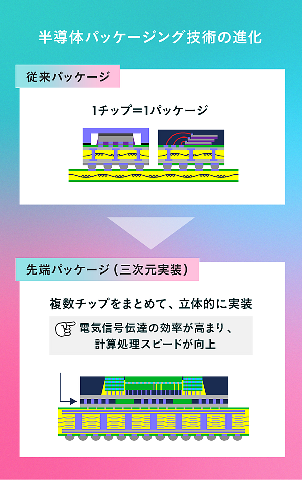
The latest technology in the packaging process is " 3D packaging ."
This technology vertically stacks and connects multiple semiconductor chips, shortening the distance between chips and increasing the efficiency of data transfer, thereby improving semiconductor performance.
── Is the vertical stacking of chips a technological innovation?
Yamaguchi : Yes. The cutting-edge semiconductors mass-produced at TSMC have circuit line widths as small as 3nm (nanometers).
These tiny semiconductors must be stacked and then tightly overlapped to ensure electrical connection.
From material selection to precise alignment and heat management, a wide range of highly advanced technologies are required.
YasuharaWhat 's even more difficult is that unless there is a certain yield, the business won't be viable.
I am in charge of process development at our center, and because we handle very expensive semiconductor chips, we need to do everything we can to reduce defective products in the packaging process.
Therefore, inspection techniques that prevent defective products from being produced or detect them at the earliest possible stage are also important .
Semiconductor manufacturing is a kind of "comprehensive art."
Just like movies or operas, it can only be created by mobilizing a group of engineers with a wide range of specialized knowledge, from materials chemistry, mechanical engineering, and thermal engineering to information control.
The Emoto Center is a base for research and development of materials and equipment technologies related to advanced packaging technology in collaboration with Japanese suppliers (companies that provide parts and materials).
Japanese companies hold top global market shares for many semiconductor materials and equipment products.
Through research and development that leverages the strengths of Japanese companies, we hope to create technology that meets the cutting-edge needs of the semiconductor industry.
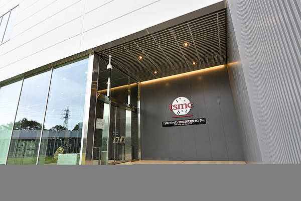
TSMC Japan 3DIC Research and Development Center in Tsukuba City. Photo courtesy of TSMC.
--It seems like there are benefits for suppliers as well by collaborating with this center.
Emoto : Yes. I believe that through collaboration with TSMC, Japanese suppliers can hone their unique technological capabilities and share them with the world .
TSMC is a "dedicated foundry" that does not have its own products but specializes in manufacturing products ordered by customers, and works with customers around the world to create cutting-edge, innovative products.
Therefore, by partnering with TSMC, Japanese material and equipment manufacturers can keep up with the latest trends and needs in the semiconductor market , enabling them to sell products and technologies that meet market demand worldwide.
Therefore, at our center, we interpret the specifications required by our global customers as TSMC, and then ask our Japanese suppliers specifically, "Can you make materials with these characteristics?"
We believe that by engaging in these types of discussions and making adjustments, we can provide value to the research and development efforts of our suppliers.
Yamaguchi: Another advantage for Japanese companies is that their products may be adopted by TSMC.
In typical semiconductor device manufacturers, the research and development department is separate from the manufacturing and mass production department, so even if good results are obtained in the research stage, they often produce different results in mass production, resulting in rework.
In contrast, the prototype line installed at our center corresponds to that at our headquarters factory , so the results obtained can be directly reflected on the mass production line in Taiwan.
There is no "game of telephone" between the headquarters and our center, which is why we can move from research and development and prototyping to mass production much faster.
Emoto: Once we actually started operations, the benefits of being based in Japan were greater than we had imagined.
When the center first opened, it collaborated with around 40 Japanese companies, but now it is working on joint development with around 120 companies.
Although initially it was largely experimental, as we began to see results, the research and development themes expanded, and we have been able to expand the scope of our collaboration with more companies.
Yasuhara: In fact, we're also receiving more inquiries from our headquarters in Taiwan. We're receiving a lot of specific requests, such as, "Can you solve these problems?" or "Could you try out new technologies together with our Japanese suppliers?" and we can really feel the high expectations.
Emoto: To give one specific example, right after our center opened, demand for 3D packaging products exploded, and there was a time when our Taiwan headquarters had to quickly increase its production capacity.
Factories faced various challenges in expanding mass production, but our center collaborated with Japanese manufacturers to identify the causes of defects caused by materials and contributed to resolving the mass production issues.
On the other hand, it is also true that Japanese companies are being asked to act with even greater speed . The strengths that Japanese companies currently possess in the fields of materials and equipment are by no means secure.
Overseas, rapidly growing material and equipment manufacturers are emerging one after another. Japanese companies need to act faster to protect and further expand the market share they have built up to now.
TSMC is committed to rapid decision-making and R&D to meet customer product innovation needs in a timely manner.
We believe that collaborating with our Japanese partners and suppliers and advancing research and development of materials and equipment at the same pace will further hone Japan's strengths in the materials and equipment fields and lead to the development of Japan's semiconductor industry.
YasuharaThe role of our center is to act as a bridge connecting companies with outstanding technology in Japan's semiconductor ecosystem with the global semiconductor market .
We hope that Japanese material and equipment-related companies will view this center as a gateway to the global market and make full use of it.
When we work together on research and development, we don't care about the size of the company. We want to connect with companies in the semiconductor field that have solid technological capabilities.
Emoto: The semiconductor field is changing at an incredible pace. We believe that our ability to pioneer this frontier together with Japanese companies is a major strength.
We will continue to work at full speed to ensure that this base produces a steady stream of new technologies and outstanding human resources, and that it can demonstrate its presence on the global stage.
Written by: Etsuko Morita
Photography by: Masahiro Kojima
Design by: Kotoko Honda
Edited by: Asuka Kanai

 newspicks.com
TSMC, a Taiwanese semiconductor contract manufacturer, has been strengthening its research and development in back-end manufacturing over the past decade.
It may not be widely known that TSMC has established a research and development center for advanced packaging technology in Tsukuba, Japan. However, the foundation for co-creation with Japanese companies has already been laid.
Why is TSMC based in Japan and promoting collaboration with Japanese companies? We spoke with Yutaka Emoto, director of the TSMC Japan 3DIC Research and Development Center (hereinafter referred to as the 3DIC Research and Development Center), the center's base; Shinpei Yamaguchi , who leads materials development on-site; and Ryutaro Yasuhara , who is responsible for process development .
Semiconductor manufacturing is a "comprehensive art"
──Traditionally, the main focus of semiconductors has been the "front-end process," which improves performance through miniaturization, but in recent years, attention has been focused on the more downstream "back-end process."Emoto : Yes, that's right. I am the director of the research and development center for this "post-processing" but I actually don't like the term "post-processing."
Traditionally, downstream processes in manufacturing have been considered to be little more than "assembling finished parts," and have been considered less technically difficult than upstream processes.
However, the cutting edge of semiconductor manufacturing today is something completely different from "simple assembly work." It has evolved into the field of "advanced packaging," which requires extremely advanced technology.
Why did this evolution occur?
Yamaguchi : Simply put, it's because the computing power required of semiconductors has increased dramatically.
To take a recent example, the rise of generative AI has increased the need for high-performance semiconductors, and we are now in a situation where technological innovation in the front-end process alone is no longer enough.
I am personally involved in materials research and development at the 3DIC Research and Development Center, and I feel every day that innovation is required even in the packaging process that brings together semiconductor chips.
The latest technology in the packaging process is " 3D packaging ."
This technology vertically stacks and connects multiple semiconductor chips, shortening the distance between chips and increasing the efficiency of data transfer, thereby improving semiconductor performance.
── Is the vertical stacking of chips a technological innovation?
Yamaguchi : Yes. The cutting-edge semiconductors mass-produced at TSMC have circuit line widths as small as 3nm (nanometers).
These tiny semiconductors must be stacked and then tightly overlapped to ensure electrical connection.
From material selection to precise alignment and heat management, a wide range of highly advanced technologies are required.
YasuharaWhat 's even more difficult is that unless there is a certain yield, the business won't be viable.
I am in charge of process development at our center, and because we handle very expensive semiconductor chips, we need to do everything we can to reduce defective products in the packaging process.
Therefore, inspection techniques that prevent defective products from being produced or detect them at the earliest possible stage are also important .
Semiconductor manufacturing is a kind of "comprehensive art."
Just like movies or operas, it can only be created by mobilizing a group of engineers with a wide range of specialized knowledge, from materials chemistry, mechanical engineering, and thermal engineering to information control.
Why TSMC is establishing its R&D center in Tsukuba
──TSMC established the 3DIC Research and Development Center in Tsukuba City in 2021, a research and development center specializing in advanced packaging technology. I heard that Japan is the first country outside of Taiwan to have such an R&D center.The Emoto Center is a base for research and development of materials and equipment technologies related to advanced packaging technology in collaboration with Japanese suppliers (companies that provide parts and materials).
Japanese companies hold top global market shares for many semiconductor materials and equipment products.
Through research and development that leverages the strengths of Japanese companies, we hope to create technology that meets the cutting-edge needs of the semiconductor industry.
TSMC Japan 3DIC Research and Development Center in Tsukuba City. Photo courtesy of TSMC.
--It seems like there are benefits for suppliers as well by collaborating with this center.
Emoto : Yes. I believe that through collaboration with TSMC, Japanese suppliers can hone their unique technological capabilities and share them with the world .
TSMC is a "dedicated foundry" that does not have its own products but specializes in manufacturing products ordered by customers, and works with customers around the world to create cutting-edge, innovative products.
Therefore, by partnering with TSMC, Japanese material and equipment manufacturers can keep up with the latest trends and needs in the semiconductor market , enabling them to sell products and technologies that meet market demand worldwide.
Therefore, at our center, we interpret the specifications required by our global customers as TSMC, and then ask our Japanese suppliers specifically, "Can you make materials with these characteristics?"
We believe that by engaging in these types of discussions and making adjustments, we can provide value to the research and development efforts of our suppliers.
Yamaguchi: Another advantage for Japanese companies is that their products may be adopted by TSMC.
In typical semiconductor device manufacturers, the research and development department is separate from the manufacturing and mass production department, so even if good results are obtained in the research stage, they often produce different results in mass production, resulting in rework.
In contrast, the prototype line installed at our center corresponds to that at our headquarters factory , so the results obtained can be directly reflected on the mass production line in Taiwan.
There is no "game of telephone" between the headquarters and our center, which is why we can move from research and development and prototyping to mass production much faster.
A bridge between Japanese companies and the global market
──What achievements have been made in the four years since the 3DIC Research and Development Center opened?Emoto: Once we actually started operations, the benefits of being based in Japan were greater than we had imagined.
When the center first opened, it collaborated with around 40 Japanese companies, but now it is working on joint development with around 120 companies.
Although initially it was largely experimental, as we began to see results, the research and development themes expanded, and we have been able to expand the scope of our collaboration with more companies.
Yasuhara: In fact, we're also receiving more inquiries from our headquarters in Taiwan. We're receiving a lot of specific requests, such as, "Can you solve these problems?" or "Could you try out new technologies together with our Japanese suppliers?" and we can really feel the high expectations.
Emoto: To give one specific example, right after our center opened, demand for 3D packaging products exploded, and there was a time when our Taiwan headquarters had to quickly increase its production capacity.
Factories faced various challenges in expanding mass production, but our center collaborated with Japanese manufacturers to identify the causes of defects caused by materials and contributed to resolving the mass production issues.
On the other hand, it is also true that Japanese companies are being asked to act with even greater speed . The strengths that Japanese companies currently possess in the fields of materials and equipment are by no means secure.
Overseas, rapidly growing material and equipment manufacturers are emerging one after another. Japanese companies need to act faster to protect and further expand the market share they have built up to now.
TSMC is committed to rapid decision-making and R&D to meet customer product innovation needs in a timely manner.
We believe that collaborating with our Japanese partners and suppliers and advancing research and development of materials and equipment at the same pace will further hone Japan's strengths in the materials and equipment fields and lead to the development of Japan's semiconductor industry.
YasuharaThe role of our center is to act as a bridge connecting companies with outstanding technology in Japan's semiconductor ecosystem with the global semiconductor market .
We hope that Japanese material and equipment-related companies will view this center as a gateway to the global market and make full use of it.
When we work together on research and development, we don't care about the size of the company. We want to connect with companies in the semiconductor field that have solid technological capabilities.
Emoto: The semiconductor field is changing at an incredible pace. We believe that our ability to pioneer this frontier together with Japanese companies is a major strength.
We will continue to work at full speed to ensure that this base produces a steady stream of new technologies and outstanding human resources, and that it can demonstrate its presence on the global stage.
Written by: Etsuko Morita
Photography by: Masahiro Kojima
Design by: Kotoko Honda
Edited by: Asuka Kanai
TSMCとの共創は、なぜ日本企業の「絶好のチャンス」なのか
──従来の半導体の主役は、微細化で性能を高める「前工程」でしたが、より下流の「後工程」に近年注目が集まっていますね。江本 ええ。私はその「後工程」の研究開発拠点でセンター長を務めていますが、実は...