You are currently viewing SemiWiki as a guest which gives you limited access to the site. To view blog comments and experience other SemiWiki features you must be a registered member. Registration is fast, simple, and absolutely free so please, join our community today!
Shrinkage has come to an end, will it be stacking, increase in energy efficiency, production processes or maybe even cost reductions? Are there any radical changes at all on the horizon?
Near term: advanced packaging, chiplets, 3D stacking.
Medium term: silicon photonics, CPO.
Long term: AI robots organize matter through telepathy displacing the need for fabs and manufacturing while we sit on the beach and sip drinks.
Logic - the IMEC roadmap now goes out to 2039 with newer transistor types coming. We're transitioning from FinFET to GAAFET now (also known as Nanosheet), the IMEC roadmap shows "CFET" around 2031 (7A process?), and "2DFET?" as the next type around 2037 or so (2A process tentatively). That indicates about 6 years / 3 "nodes" per transistor type, compared to ~ a really long time for Planar, and ~ 13 years for FinFET.
2D materials are promising to extend the logic technology roadmap, but developments are needed towards industrial adoption. Read about imec’s unique approach.
www.imec-int.com
I think NAND / Flash memory still has some headroom to go with cell changes (5-6 levels per cell) on top of more 3D stacking.
As far as the machinery goes -- High NA and "Hyper NA" are in development. Pat Gelsinger has indicated High NA may help lower costs per transistor, though a lot of others here have disagreed (with good arguments from what I understand).
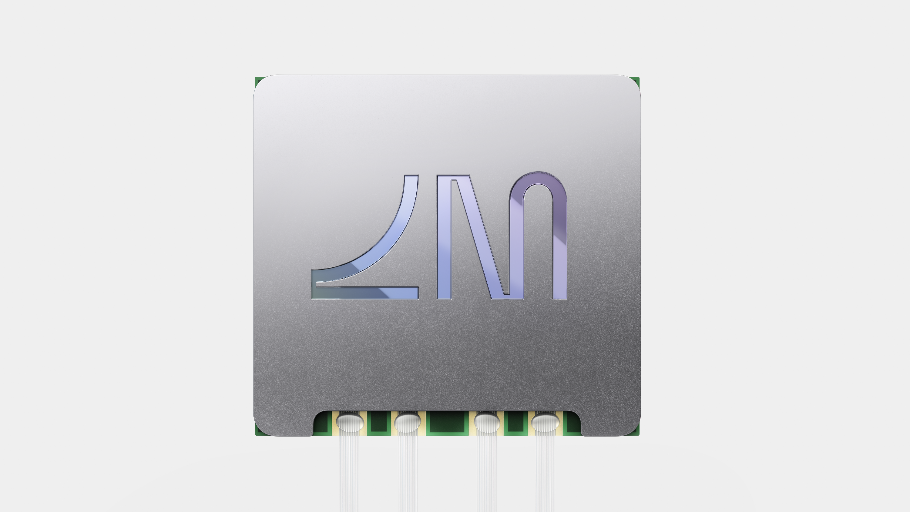
I do wonder if we will see the optical computing that was promised by LightMatter and others a few years ago. LightMatter still has their original photonic technology on their books in their Envise research, but the company has mainly pivoted to CPO for current revenue.
Discover Envise™ the world’s first photonic computing platform for AI, offering unmatched performance and energy efficiency to power next-gen neural networks.
I'd like to hear from anyone knowledgable on 'compute in memory' - are there any products/solutions in the works here that would be revolutionary for some use cases?
") -- New processes are already requiring many USD $B to come to market..
-- New processes are already requiring many USD $B to come to market..