fansink
Well-known member
Production at Fab 21 module 2 is set to start at least two quarters earlier.
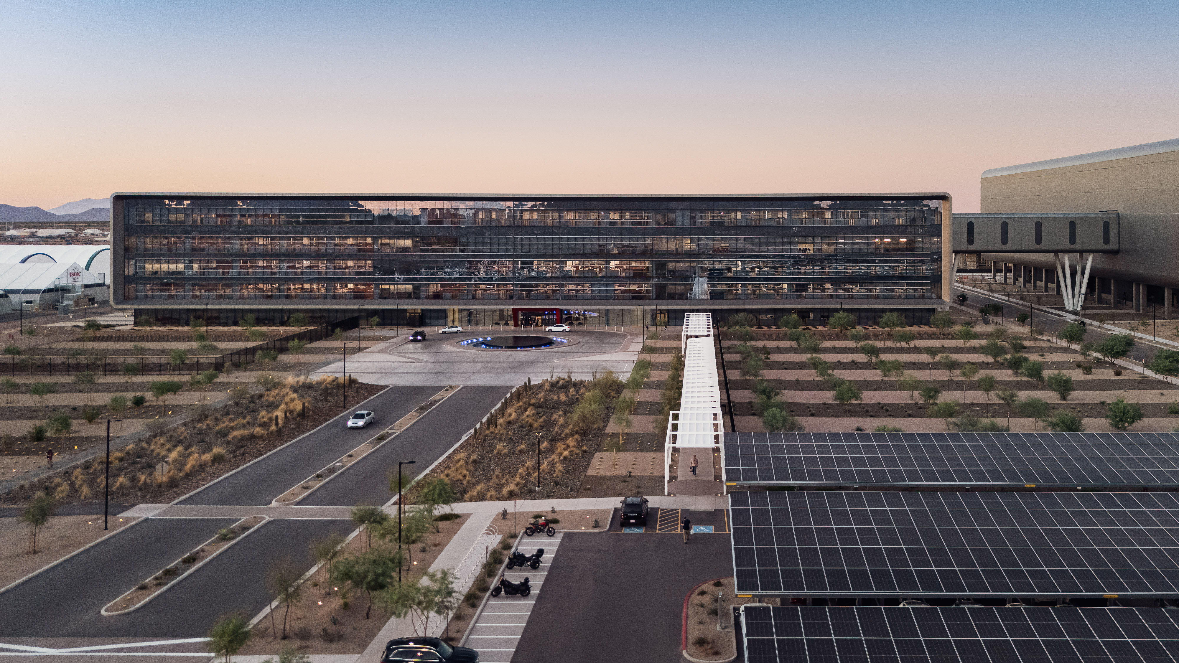
TSMC plans to produce 30% of its N2 (2nm-class) output in the U.S. and make its Fab 21 site near Phoenix, Arizona, an independent semiconductor manufacturing cluster, the company's management revealed during the company's earnings call on Thursday. The world's largest contract maker of chips also indicated intentions to speed up building new Fab 21 modules to produce chips on N3 (3nm-class), N2, and A16 (1.6nm-class) nodes.
"After completion, around 30% of our 2nm and more advanced capacity will be located in Arizona, creating an independent leading edge semiconductor manufacturing cluster in the U.S.," said C.C. Wei, chief executive and chairman of TSMC, in his prepared remarks. "It will also create greater economies of scale and help foster a more complete semiconductor supply chain ecosystem in the U.S."
To produce 30% of its N2 and A16 output in Arizona, TSMC will build two additional Fab 21 modules. So far, the company has confirmed plans to build at least three N2 and A16-capable fab modules in Taiwan's Hsinchu and Kaohsiung Science Parks with more modules incoming, so the island will still produce the lion's share of TSMC's advanced chips. Yet, 30% of TSMC's N2 and A16 chips produced in the U.S. is certainly a big deal.
TSMC's Fab 21 module 1 in Arizona is currently ramping up volume production of chips for its American customers using the company's N4 and N5 process technologies. Construction of the company's N3-capable Fab 21 module 2 (its second fabrication facility in Arizona) is complete, and the company is working to start installing equipment there ahead of time in a bid to pull in volume production of chips at the facility by at least a couple of quarters from its original vague schedule of 2028.
Construction of Fab 21 module 3 and module 4 — the company's facilities that will use N2 and A16 nodes — is expected to start later this year, assuming all required permits are obtained. TSMC did not reveal schedules for these Fab 21 modules, but it is reasonable to expect at least one of them to come online by early 2029 provided that TSMC acquires all the necessary equipment on time.
TSMC's Fab 21 module 5 and module 6 will use process technologies beyond A16 (think A14 and possibly more advanced), but their construction timelines and production ramp will depend on future customer demand.
TSMS's grand plan for Fab 21 is to evolve it into a GigaFab cluster with production capacity of at least 100,000 wafer starts per month, though when exactly this happens is something that remains to be seen.
"Our expansion plan will enable TSMC to scale up to a GigaFab cluster to support the needs of our leading-edge customers in smartphone, AI and HPC applications," added Wei.
 www.tomshardware.com
TSMC plans to produce 30% of its N2 (2nm-class) output in the U.S. and make its Fab 21 site near Phoenix, Arizona, an independent semiconductor manufacturing cluster, the company's management revealed during the company's earnings call on Thursday. The world's largest contract maker of chips also indicated intentions to speed up building new Fab 21 modules to produce chips on N3 (3nm-class), N2, and A16 (1.6nm-class) nodes.
"After completion, around 30% of our 2nm and more advanced capacity will be located in Arizona, creating an independent leading edge semiconductor manufacturing cluster in the U.S.," said C.C. Wei, chief executive and chairman of TSMC, in his prepared remarks. "It will also create greater economies of scale and help foster a more complete semiconductor supply chain ecosystem in the U.S."
To produce 30% of its N2 and A16 output in Arizona, TSMC will build two additional Fab 21 modules. So far, the company has confirmed plans to build at least three N2 and A16-capable fab modules in Taiwan's Hsinchu and Kaohsiung Science Parks with more modules incoming, so the island will still produce the lion's share of TSMC's advanced chips. Yet, 30% of TSMC's N2 and A16 chips produced in the U.S. is certainly a big deal.
TSMC's Fab 21 module 1 in Arizona is currently ramping up volume production of chips for its American customers using the company's N4 and N5 process technologies. Construction of the company's N3-capable Fab 21 module 2 (its second fabrication facility in Arizona) is complete, and the company is working to start installing equipment there ahead of time in a bid to pull in volume production of chips at the facility by at least a couple of quarters from its original vague schedule of 2028.
Construction of Fab 21 module 3 and module 4 — the company's facilities that will use N2 and A16 nodes — is expected to start later this year, assuming all required permits are obtained. TSMC did not reveal schedules for these Fab 21 modules, but it is reasonable to expect at least one of them to come online by early 2029 provided that TSMC acquires all the necessary equipment on time.
TSMC's Fab 21 module 5 and module 6 will use process technologies beyond A16 (think A14 and possibly more advanced), but their construction timelines and production ramp will depend on future customer demand.
TSMS's grand plan for Fab 21 is to evolve it into a GigaFab cluster with production capacity of at least 100,000 wafer starts per month, though when exactly this happens is something that remains to be seen.
"Our expansion plan will enable TSMC to scale up to a GigaFab cluster to support the needs of our leading-edge customers in smartphone, AI and HPC applications," added Wei.
TSMC to build 30% of its 2nm and more advanced chips in the U.S., to speed up Fab 21 build out
Production at Fab 21 module 2 is set to start at least two quarters earlier.