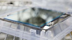
TSMC is repurposing its old, wound-down, 8-inch Fab 3 in Hsinchu Science Park to produce extreme ultraviolet pellicles, bringing this production in-house. An EUV pellicle is a thin, highly transparent membrane stretched above a photomask to prevent particles from contacting the mask during EUV exposure. It is designed to withstand intense EUV radiation and thermal stress while minimizing optical absorption and wavefront distortion.
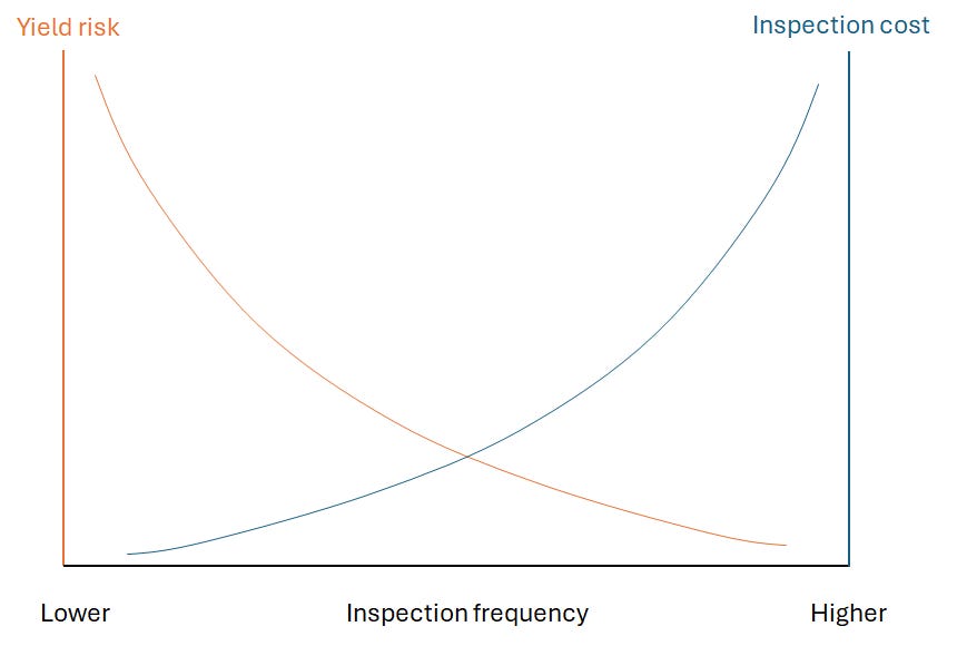
Producing pellicles is a way to shorten replacement cycles and exert more control over a component that, in EUV environments, must protect photomasks from particles while coping with extreme exposure conditions. Unlike older DUV processes, EUV systems operate with 400 W light sources and localized heating that can approach 1,000°C at the mask, increasing contamination risks and making pellicle performance more influential to wafer yields.
The economics around pellicles have encouraged divergent approaches. DUV pellicles are relatively inexpensive, at about $600, which has enabled their widespread use in earlier nodes. However, EUV variants have recorded prices near $30,000, which is a step increase that has deterred some chipmakers from blanket deployment and may have contributed to documented yield gaps.
By internalizing production, TSMC wants to achieve lower per-unit costs and more predictable supply, making pellicle integration viable at scale. That financial case goes hand in hand with materials research: carbon nanotube membranes are the most promising candidate to meet the twin demands of durability and optical transparency. Membranes must resist accelerated degradation from stronger light sources while minimizing absorption that would reduce exposure efficiency. TSMC plans to validate solutions as it ramps N2 and A16 process technologies, where improved pellicle performance could significantly boost yields and preserve its edge on advanced nodes.
Here is an explainer of what EUV pellicles are used for:

Producing pellicles is a way to shorten replacement cycles and exert more control over a component that, in EUV environments, must protect photomasks from particles while coping with extreme exposure conditions. Unlike older DUV processes, EUV systems operate with 400 W light sources and localized heating that can approach 1,000°C at the mask, increasing contamination risks and making pellicle performance more influential to wafer yields.
The economics around pellicles have encouraged divergent approaches. DUV pellicles are relatively inexpensive, at about $600, which has enabled their widespread use in earlier nodes. However, EUV variants have recorded prices near $30,000, which is a step increase that has deterred some chipmakers from blanket deployment and may have contributed to documented yield gaps.
By internalizing production, TSMC wants to achieve lower per-unit costs and more predictable supply, making pellicle integration viable at scale. That financial case goes hand in hand with materials research: carbon nanotube membranes are the most promising candidate to meet the twin demands of durability and optical transparency. Membranes must resist accelerated degradation from stronger light sources while minimizing absorption that would reduce exposure efficiency. TSMC plans to validate solutions as it ramps N2 and A16 process technologies, where improved pellicle performance could significantly boost yields and preserve its edge on advanced nodes.

Here is an explainer of what EUV pellicles are used for:
TSMC Repurposing Old Fabs to Bring EUV Pellicle Production In-House
TSMC is repurposing its old, wound-down, 8-inch Fab 3 in Hsinchu Science Park to produce extreme ultraviolet pellicles, bringing this production in-house. An EUV pellicle is a thin, highly transparent membrane stretched above a photomask to prevent particles from contacting the mask during EUV...
www.techpowerup.com