TSMC introduced a 38.1Mb/mm2 SRAM in 2nm-CMOS-nanosheet technology for high-density and energy-efficient compute applications. The design uses a 0.021um2 high-density bitcell, and through DTCO improves the overall SRAM density by 1.1× compared to the previous technology node.
This cell size is the same as N5 and N3E, as well as Intel 18A.
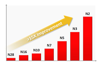

") ), that GAAFET should allow some SRAM density improvements ovef FinFET.
), that GAAFET should allow some SRAM density improvements ovef FinFET.