Please note that this article cites information from The Elec and Sisa Journal.
According to The Elec, citing industry sources, Samsung is outsourcing the production of photomasks — vital components in chipmaking — for the first time. As the report indicates, Samsung is said to be outsourcing lower-end photomasks for memory chips, signaling a strategy to channel resources toward ArF and EUV mask production.Earlier this month, Samsung reportedly placed an order with PKL, a subsidiary of U.S. photomask maker Photronics, to supply i-line and KrF photomasks for memory production. The report adds that Japan’s Tekscend Photomask is also under evaluation and expects to receive an order soon.
The report points out that, since these are masks for low-end chips, Samsung considers them to pose little risk of technology leakage. Still, producing the masks in-house remains cheaper than outsourcing, as the report notes.
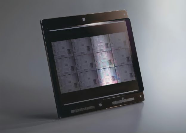
As the report highlights, photomasks transfer circuit patterns onto wafers using light and are classified by the wavelength applied. i-line uses a 365-nanometer (nm) wavelength for simple designs; KrF at 248 nm enables mid-level resolution; ArF at 193 nm supports more advanced patterns; and EUV, or extreme ultraviolet, at 13.5 nm is used for the most advanced designs.
Notably, the number of photomasks required by chipmakers is rising. While DRAM once needed only 30 to 40 masks, advanced DRAMs now use more than 60, driven by techniques such as multi-patterning, as the report points out.
The report, citing sources, states that South Korea’s photomask market was worth around the mid-700 billion won range last year. Domestic photomask makers are running their factories at over 90% capacity, with order books already full. As a result, the report suggests Samsung’s decision to outsource photomask production could make it harder for rival foundries to secure supply.
Samsung’s Push into Photomask R&D for Logic Chips
Samsung has also been advancing R&D in photomask technology. According to Sisa Journal, the company is accelerating the adoption of Phase Shift Mask (PSM) in logic semiconductor production. PSM improves the precision of wafer circuit patterns by adjusting the phase of light during exposure. Samsung is reportedly developing ways to apply PSM to processes with EUV lithography. As the report indicates, with photolithography now reaching 3nm and below, the adoption of PSMs with phase-shift layers is becoming increasingly essential.
https://www.trendforce.com/news/202...-busan-annual-output-projected-at-30k-wafers/
- © 2025 TrendForce Corp. All rights reserved