Array
(
    [content] => 
    [params] => Array
        (
            [0] => /forum/threads/samsung-foundry-faces-yield-struggles-and-client-losses-external-push-for-spinoff-and-u-s-listing.21137/page-2
        )

    [addOns] => Array
        (
            [DL6/MLTP] => 13
            [Hampel/TimeZoneDebug] => 1000070
            [SV/ChangePostDate] => 2010200
            [SemiWiki/Newsletter] => 1000010
            [SemiWiki/WPMenu] => 1000010
            [SemiWiki/XPressExtend] => 1000010
            [ThemeHouse/XLink] => 1000970
            [ThemeHouse/XPress] => 1010570
            [XF] => 2021770
            [XFI] => 1050270
        )

    [wordpress] => /var/www/html
)

Samsung Foundry Faces Yield Struggles and Client Losses, External Push for Spinoff and U.S. Listing

Very much agreed.

It should be enough. IFS's gola is to have external customers account for approximately one-third of its revenue, which should be sufficient for its biz model.

Currently, there's a widespread assumption that TSMC will maintain its technical leadership indefinitely without any significant missteps. However, how long can this assumption be held true? For instance, SemiAnalysis reports that while TSMC's backside power implementation is more advanced than IFS's PowerVia technology, it is also more complex and potentially carries higher risks. This highlights that even industry leaders can face technical challenges and uncertainties.

Which is precisely why TSMC is introducing BSPD as a "second-step" 2nm process (now called A16) after introducing GAA in 2nm (which is pretty much 3nm metal with new transistors underneath) -- do one big new thing at a time to reduce risk, and so it's not a total disaster if things get delayed or have problems. Which is where Intel fell over with 10nm, trying to do too many radical changes all at the same time, they tried to do a massive leap forwards and fell over... :-(

I expect A16 will be a "pipecleaner" for BSPD like N7+ was for EUV -- and for the same reason, not so many customers because of increased risk (perceived or real) with new technologies and that layouts/libraries are not compatible with N2 so there's no quick/easy switchover in either direction. Once BSPD has been thoroughly debugged and derisked by A16 it'll be adopted much more widely (in A14?), like N5 was as the first big-EUV process following the N7+ pipecleaner.
 
That's certainly all true about the potential for missteps. But there's quite a large AND function in this. For TSMC to lose leadership requires:

( significant misstep OR miss significant new technology ) AND competitor who doesn't AND competitor who has the resources and other attributes to replace TSMC

plus perhaps some other factors I missed.

Recent form also suggests that TSMC's more collaborative working model (I asusme they work very closely with major customers in solving problems) makes TSMC less prone to the first factor than Intel. Intel is also weaker on the last point today.

Suggests to me that TSMC really have to miss some critical new technology very badly in order to throw it away from here.

Standing well back from the detail, you do wonder if Intel's best approach isn't to aim for particular market segments rather than try to immediately confront TSMC across the whole market (never attack a much larger force head on, choose your strongest ground). Which is precisely what they are doing with 18A - though it appears more by necessity/accident than design. But the critical question as @Artificer60 says is whether even a juicy high margin, high performance market segment can be big enough today.
I was not suggesting TSMC losing its lead permanently, which IMO is unlikely. However, if it stumbles for 2 years, fabless chip designers will be prompted to diversify more into "non TSMC" foundries.
 
FuriosaAI, DeepX, and Mobilint “Choose Foundry for Chip Optimization”

Major domestic AI semiconductor fabless companies that used Samsung Electronics' foundry fabs are diversifying their foundries by also using TSMC fabs for new chip mass production.

According to the industry on the 2nd, Furiosa AI's 1st generation chip 'Warboy' used Samsung Electronics' 14nm process, but its 2nd generation chip 'Renegade' chose TSMC's 5nm process. Warboy was released in 2021 and entered mass production in April of last year, while Renegade was released in August of this year and is scheduled for mass production next year. In particular, Renegade garnered attention from the industry as the first in the domestic AI semiconductor industry to be equipped with HBM3 memory based on CoWoS, a 2.5D packaging technology. Furiosa AI's next-generation chip 'Renegade S', which is aiming for release in the 4th quarter, is also expected to choose TSMC's 5nm process.

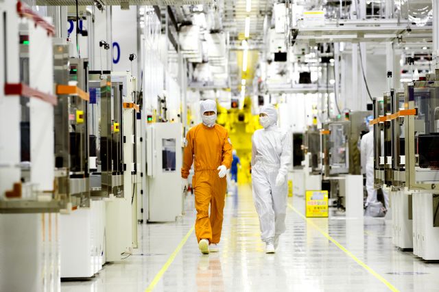
insight_FnltZgPITMro.jpg


Samsung Electronics semiconductor production site. (Photo = Samsung Electronics)

Following its use of Samsung Electronics Foundry's process , DeepX's newly developed chip this year uses the TSMC process . The 'DX-V3' SoC (system-on-chip) developed by DeepX this year utilizes TSMC's 12nm process and aims to release samples within the year. DeepX's previously released 'DX M1 (AI accelerator)' and 'DX-H1 (AI server accelerator)' are each produced using Samsung Electronics Foundry's 5nm process, while 'DX-V1 (AI SoC solution)' is produced using Samsung Electronics' 28nm process. Of these, the DX-M1 was the first to enter mass production last month. In addition, DeepX is known to be discussing the development of new chips using a more advanced process than 5nm with Samsung Electronics Foundry.

Mobilint also uses both Samsung Electronics and TSMC foundries. The first-generation chip, 'Eris', began mass production in March using Samsung Electronics' 14nm process. The second-generation chip, 'Regulus', is produced using TSMC's 12nm process and is currently being tested with the aim of launching next year.

A semiconductor industry insider explained, “AI semiconductors are an industry that requires hundreds of billions of won from development to mass production, and the survival of a company depends on the mass production of a single chip. Therefore, companies are choosing a foundry process that can optimize the chip.”

 
SemiAnalysis reports that while TSMC's backside power implementation is more advanced than IFS's PowerVia technology,
IIRC, TSMC's first iteration of fin-fet was also superior to Intel's first gen, though just like BSPD seems to be this time. Intel's 2nd gen fin-fet was much improved and I expect the same to be true for 2nd gen PSBD which I would think would be part of the 14A package. A full technode of yield learning goes a long way to improving enhancements in the next gen.
 
Which is precisely why TSMC is introducing BSPD as a "second-step" 2nm process (now called A16) after introducing GAA in 2nm (which is pretty much 3nm metal with new transistors underneath) -- do one big new thing at a time to reduce risk, and so it's not a total disaster if things get delayed or have problems. Which is where Intel fell over with 10nm, trying to do too many radical changes all at the same time, they tried to do a massive leap forwards and fell over... :-(
That was also the rational for Intel's 5N4Y. Avoid doing too many big changes in one process, to reduce risks. But obviously, this also increased R&D expenses for Intel.

Note that, even piece meal approach has risks and uncertainties. Missteps are a matter of when, not if. "Non tsmc" companies just need to keep themselves up, and wait for the when. Customers will change their minds and plans accordingly.
 
IIRC, TSMC's first iteration of fin-fet was also superior to Intel's first gen, though just like BSPD seems to be this time. Intel's 2nd gen fin-fet was much improved and I expect the same to be true for 2nd gen PSBD which I would think would be part of the 14A package. A full technode of yield learning goes a long way to improving enhancements in the next gen.

Intel was first out with FinFETs at 14nm so TSMC had a lot to learn from. TSMC first went to double patterning at 20nm then added FinFETs to it for 16nm. At that time Intel 14nm(+) was superior.

TSMC did the same thing with BSPD. Intel went first and I have no doubt TSMC will do it better because they have the top customers behind them figuring out the best was to implement it with a minimum amount of risk.

It really isn't a fair competition when TSMC has 90%+ of the customers and the entire design ecosystem collaborating with them.
 
Which is precisely why TSMC is introducing BSPD as a "second-step" 2nm process (now called A16) after introducing GAA in 2nm (which is pretty much 3nm metal with new transistors underneath) -- do one big new thing at a time to reduce risk, and so it's not a total disaster if things get delayed or have problems. Which is where Intel fell over with 10nm, trying to do too many radical changes all at the same time, they tried to do a massive leap forwards and fell over... :-(

I expect A16 will be a "pipecleaner" for BSPD like N7+ was for EUV -- and for the same reason, not so many customers because of increased risk (perceived or real) with new technologies and that layouts/libraries are not compatible with N2 so there's no quick/easy switchover in either direction. Once BSPD has been thoroughly debugged and derisked by A16 it'll be adopted much more widely (in A14?), like N5 was as the first big-EUV process following the N7+ pipecleaner.

There is an important aspect of the "pipe cleaner" in the semiconductor industry that we need to pay attention to: the cost. If a "pipe cleaner" process node is placed on a company's roadmap and has product delivery tied to it, then it becomes serious business with significant implications and consequences.

In the case of Intel's 20A, a pipe cleaner for Intel 18A, it was canceled by Intel and didn't enter high-volume production. Intel stated that this was because progress on 18A was so great that 20A became unnecessary. Intel also stated that canceling 20A and shifting engineering resources to 18A would save the company $500 million.

What Intel didn’t mention is how much money was lost due to the 20A. Although a portion of 20A's development and manufacturing preparation can be used for 18A, I suspect a significant amount was simply a loss. A pipe cleaner node that fails to enter high volume production becomes a very expensive "pipe cleaner".
Agreed, but there's a big difference between a complete Intel-style flop and a TSMC-style pipecleaner... ;-)

I'm confident that A16 will get into mass production, probably with a relatively small number of designs but some of these (Apple?) will be big volume -- basically, customers with big balls and deep pockets who are willing to take the BSPD risk to gain a performance advantage, the "bleeding-edge" adopters.

But many more risk-averse customers will wait to see that A16 actually delivers (PPA, yield, cost) before jumping on the BSPD bandwagon, in the meantime they'll stick with N2 -- and by the time all this is proven A14 will be coming along soon, and since they need to relayout everything for BSPD they'll probably go for A14 not A16 because it's now a better fit to their timescales.

Bear in mind that BSPD in A16 is a difficult-to-do but relatively low-cost "add-on" to N2, all the other hard bits which affect yield like the transistors and the metal stack (with EUV masks and tight layout rules) have already been de-risked, and that's where most of the process development investment goes.

I did not think the first GAA nodes would be big for the same reason. TSMC N3 did so well why not stick with it until N2 is pipe cleaned? TSMC clearly stated that N2 has as many tape outs as N3 at this period in time. At the most recent TSMC event LC Lui shared some DTCO numbers:

TSMC DTCO Innovation.jpg
 
Agreed, but there's a big difference between a complete Intel-style flop and a TSMC-style pipecleaner... ;-)

I'm confident that A16 will get into mass production, probably with a relatively small number of designs but some of these (Apple?) will be big volume -- basically, customers with big balls and deep pockets who are willing to take the BSPD risk to gain a performance advantage, the "bleeding-edge" adopters.

But many more risk-averse customers will wait to see that A16 actually delivers (PPA, yield, cost) before jumping on the BSPD bandwagon, in the meantime they'll stick with N2 -- and by the time all this is proven A14 will be coming along soon, and since they need to relayout everything for BSPD they'll probably go for A14 not A16 because it's now a better fit to their timescales.

Bear in mind that BSPD in A16 is a difficult-to-do but relatively low-cost "add-on" to N2, all the other hard bits which affect yield like the transistors and the metal stack (with EUV masks and tight layout rules) have already been de-risked, and that's where most of the process development investment goes.

"Agreed, but there's a big difference between a complete Intel-style flop and a TSMC-style pipecleaner... ;-)"


For a pure-play foundry like TSMC, it cannot afford to cancel a process node and simply tell customers to move to the latest and greatest future technology. With so many dreams, hopes, and hundreds of millions of dollars at stake from customers who have entrusted TSMC, such thing is not feasible.

For an IDM like Intel, it’s a different story.
 
I did not think the first GAA nodes would be big for the same reason. TSMC N3 did so well why not stick with it until N2 is pipe cleaned? TSMC clearly stated that N2 has as many tape outs as N3 at this period in time. At the most recent TSMC event LC Lui shared some DTCO numbers:

View attachment 2330

Do you think this has something to do with the recent AI investment boom? Companies want to gain a bit edge, at whatever cost.

I certainly think so.
 
For an IDM like Intel, it’s a different story.
I agree. 5N4Y was expensive and not sustainable. The fact that Intel only intended to run a fraction of Arrow Lake production on the node made it a poor economic choice to ramp. Had Intel decided to move to 20A and push out 18A I would have considered that far more of a red flag. I have trouble seeing Intel not to choose to ramp 20A as a big deal. It was never going to make them money.
 
I did not think the first GAA nodes would be big for the same reason. TSMC N3 did so well why not stick with it until N2 is pipe cleaned? TSMC clearly stated that N2 has as many tape outs as N3 at this period in time. At the most recent TSMC event LC Lui shared some DTCO numbers:

View attachment 2330

Because moving from N2 to A16 needs a much bigger investment in IP and layout/tools than moving from N3 to N2, and is pretty much a one-way transition (difficult to reverse)?

N2 is pretty much N3 with a different transistor dropped in underneath, the libraries and IP and power grid/routing (where a lot of the effort goes) are otherwise quite similar -- porting layouts from one to the other is pretty easy (and reversible), and much of this is invisible to designers who don't even see the transistors, the chips look almost the same.

A16 with BSPD needs a complete rethink of libraries/tools/power grid/routing since the thick metal layers, power grid, global routing, inductors, and decoupling are all on the back side -- the resulting layouts look very different, especially IP like high-speed SERDES which take a huge time and effort to develop. And if you do all this and A16 stumbles it's difficult to go back to N2 because so much is different -- even the heat dissipation paths and self-heating. The complete change in chip structure also carries risks of reliability/assembly problems, which I'm sure will be solved (if they happen at all) but may not emerge immediately or take time to solve.

So BSPD sounds simple but it's not, as far as the end user is concerned it's a much bigger (and harder to reverse!) change than N20-N16 (FinFET) or N3-N2 (GAA) where "only" the transistors changed -- of course this is a massive change for the foundry, but hardly affects the end users -- except they get better transistors, or course... :)

Do you think TSMC A14 will be a two year node like N3 and N2, coming out 2 years after N2 and two years before A12?

Do you use DTCO? TSMC predicts double digit design gains for A16 NanoFlex for power and density versus N2 NanoFlex which is significant. So it is much bigger gains than N7 versus N7+ (first EUV and no real power/density gains)

Thanks!
 
英特尔代工厂将自己定位为台积电的竞争对手,作为技术领导者,4 年内实现 5 个节点,对吗?不幸的是,代工客户已经在 3nm 和 2nm 上投票,台积电赢得了 90% 以上的市场份额,包括英特尔自己。你真的认为这会改变吗?英特尔为什么要打一场必败的仗?你认为投资者会接受持续的亏损吗?帕特·基辛格实际上是在用这个策略抵押公司,但没有奏效。GlobalFoundries 试图用石油钱做同样的事情,谢天谢地,他们转型了,现在在非台积电市场经营着一家盈利的业务。英特尔也需要做同样的事情,转型或死亡。我已经记不清英伟达在过去 30 年里转型了多少次。我也记不清硅谷有多少家公司没有转型而倒闭了。我不希望英特尔成为其中之一。

你会建议他们怎么做?坚持下去还是转型?
2nm is a different game, yes they still have majority of customers in N2. but none of that is guaranteed they can continue to have >90% of market share l'm pretty sure, with the moving inhouse, Intel will at least get 15 % advanced market share from TSMC along with several customers.
 
英特尔代工厂将自己定位为台积电的竞争对手,作为技术领导者,4 年内实现 5 个节点,对吗?不幸的是,代工客户已经在 3nm 和 2nm 上投票,台积电赢得了 90% 以上的市场份额,包括英特尔自己。你真的认为这会改变吗?英特尔为什么要打一场必败的仗?你认为投资者会接受持续的亏损吗?帕特·基辛格实际上是在用这个策略抵押公司,但没有奏效。GlobalFoundries 试图用石油钱做同样的事情,谢天谢地,他们转型了,现在在非台积电市场经营着一家盈利的业务。英特尔也需要做同样的事情,转型或死亡。我已经记不清英伟达在过去 30 年里转型了多少次。我也记不清硅谷有多少家公司没有转型而倒闭了。我不希望英特尔成为其中之一。

你会建议他们怎么做?坚持下去还是转型?
GlobalFoundries is the one that's playing the losing battle, not Intel. They just need to make sure the manufacturing is on track, and move all if not most in house. They can still survive this way.
 
The NOT TSMC market is companies that want a second source (my definition). This included Qualcomm, Nvidia, Google, and a few other whales who used Samsung. The foundry business is very price sensitive and inherently multi source for that reason. Samsung sells wafers on price and we are talking double digit discounts from TSMC pricing.

Apple went exclusive with TSMC after using Samsung from 90nm down to 28nm. The Apple TSMC relationship started at 20nm and is what made TSMC the dominant foundry we see today, my opinion. Apple wrote some very big checks, co-developed the processes, and got first access to wafers. TSMC then developed an executive flier club for customers exclusive to TSMC. It really is the difference between flying coach and flying first class.

Samsung had competitive processes at 14nm and 7nm but 5nm and 3nm were late to yield. Samsung 5nm is yielding now so they are getting business but Samsung 3nm (the first GAA process) was a complete bust. If TSMC matches Samsung prices they will not lose customers and TSMC certainly has the margins to do it. The only issue I see is the whole monopoly problem.

What I am wondering is will the top fabless semiconductor companies swing back to multi sourcing after enjoying the perks of flying first class with TSMC?
So the thing is you have to play politics if you are CEO of Intel. You have to accuse TSMC for being monopoly. That isn't right or wrong. It's just business 101
 
I guess I'm just thick.

Is it your suggestion that Intel quit trying to provide leading edge processes? I don't think the NOT TSMC market as you define it is looking for trailing edge foundry service, but maybe I'm wrong. It is my impression the NOT TSMC market was looking to Samsung to provide an alternative at the leading edge. If Intel is to take their 11% of the market, don't they have to provide leading edge processes? Intel has never stated they intend to be the number 1 foundry option. I do recall them saying they were shooting for number 2 which would mean capturing most of Samsung's market. It seems to me that their goals and you suggestion are aligned.

I'm also curious if all of Intel's products + all of Samsung's foundry market would be enough to fund leading edge development. It seems to me that is really the crux of the matter.
Let's do a factor analysis. What does Intel consist of today? Intel Product, Intel Foundry. Majority of the current gen are outsourced to TSMC. So that $50B-$60B is taking into account factors like

What did some of the lost revenue go?
1. it is still running at a process deficit, it takes time for the newest product to ramp
2. AI training has been eating data-center revenue. But people cannot afford using all Nvidia hardware as it is expensive, and solely controlled by hyperscaler and big corporate. But AI inferencing will eventually come. All of those workloads need somewhere that is cheaper, and closer to the user.
3. People had upgraded their machines 2020- 2022. Even with AI PC, there is no much traction from the market. But the refresh cycle will eventually come.
4. Arm have become a quite dominant force in data center, some of the CPU sales were declined due to hyper-scaler develop their software based on Arm. That is revenues that may never come back to either Intel or AMD. But TSMC has been the winner for sure.

What can Intel get from TSMC?
1. future products pull in-house. This save gross margin. The product price can be increased as we are seeing with the highest price of $17k for Xeon 6P. There can be revenue growth because of more competitive products.
2. The semiconductor industry is booming, there are more opportunity for a foundry today than 10 years ago because it is now a two horses race, TSMC and IFS. There will always be some niche industry that have to use IFS to do fabrication and packaging.
3. Increasingly packaging is more important. And for Intel, there is no logarithmic growth, it is more predictable. And does not require huge lead time.
4. Intel can enter new industry, like car infotainment system. I wonder why they not partner with Mobileye on this. They can develop a chip that run on automobile.
5. They are going to monetize from deprecated assets with intel 12, Intel 16.
 
2nm is a different game, yes they still have majority of customers in N2. but none of that is guaranteed they can continue to have >90% of market share l'm pretty sure, with the moving inhouse, Intel will at least get 15 % advanced market share from TSMC along with several customers.

Intel will definitely bring their designs back inhouse for manufacturing. Intel did not sign an N2 agreement with TSMC. I do not think that Intel is currently 15% of TSMC's business. I also do not think Intel 18A will get big customers from TSMC N2. Maybe some chiplet business but not full chip which is where TSMC makes big money (Apple, QCOM, AMD, Nvidia, Broadcom, etc...).

For the A14 and 14A node battle I think it will depend on Intel's ability to implement BSPD for customers. TSMC certainly has the advantage here but it is too soon to tell. If I had to bet today it would be on TSMC and SPR. BSPD and SPR are yet another foundry differentiator that will increase the strength of TSMC's customer loyalty program.

So the thing is you have to play politics if you are CEO of Intel. You have to accuse TSMC for being monopoly. That isn't right or wrong. It's just business 101

GlobalFoundries played the "TSMC is a risk due to earthquakes and hurricanes" card when they first launched and it failed. Wishing harm on an entire country is a bad strategy. Intel did the same with the China threat. Again, not a good strategy but it did get us the CHIPs Act but that included TSMC.

Playing the monopoly card may work with the US Government and the CHIPs Act II. Unfortunately Pat sold the politicians on Intel beating TSMC at the leading edge and again that failed so I do not know how much clout he has left.

Remember, TSMC is in the position they are in today because Intel and Samsung are currently failing in the foundry business. TSMC is not dumping product. But monopoly is a good soundbite so that card will certainly play in the FUD (fear, uncertainty, and doubt) game.
 
For the A14 and 14A node battle I think it will depend on Intel's ability to implement BSPD for customers. TSMC certainly has the advantage here but it is too soon to tell. If I had to bet today it would be on TSMC and SPR. BSPD and SPR are yet another foundry differentiator that will increase the strength of TSMC's customer loyalty program.
Can you elaborate on this? BSPD is part of 18A. Customers that are running shuttles at Intel now have access to BSPD. Intel 14A will be 2nd generation BSPD for Intel. In areas like fin-fet and strained silicon Intel have been able to show significant improvement in their 2nd generation implementation. Why would you thing that this is an advantage for TSMC?
 
Back
Top