")
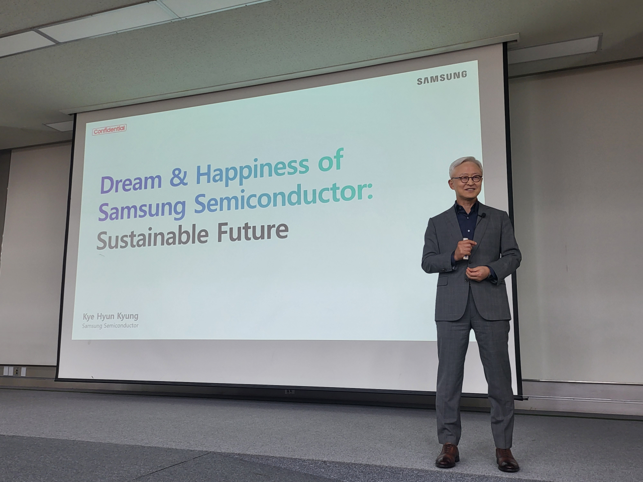
Kyung Kye-hyun, co-CEO at Samsung Electronics who is in charge of the tech giant's chip business, delivers a special lecture at Seoul National University on Tuesday. (Samsung Electronics)
Samsung Electronics co-CEO Kyung Kye-hyun, who oversees the tech giant’s chips business, expressed confidence in the foundry competition with its archrival, Taiwan Semiconductor Manufacturing Co., in line with the construction of a new chip plant in Taylor, Texas.
Kyung visited Seoul National University on Tuesday to deliver a special lecture, titled “Dream & Happiness of Samsung Semiconductor: Sustainable Future," to promising talents.
The lecture was preceded by those previously delivered to students at the Korea Advanced Institute of Science and Technology in Daejeon and Yonsei University in Seoul in May and June, respectively.
At Tuesday's lecture, the co-chief talked about his latest visit to the Taylor plant during a business trip to the US in July, and said that Samsung will start manufacturing 4-nanometer chips there by the end of next year.
Kyung expressed pride in Samsung getting ahead of TSMC, which had announced a delay in opening its advanced wafer lab in the US, despite its head start. “I felt our employees’ spirit,” Kyung said.
The chips chief emphasized that the world's largest memory chip maker is playing a “home game” in the US, while its archrival is playing an “away game” there.
According to Taiwan-based market tracker TrendForce on Wednesday, Samsung has narrowed its market share gap with TSMC by posting impressive quarterly revenue gains in the April-June period.
Samsung’s second-quarter market share in the global foundry segment rose to 11.7 percent from the previous quarter's 9.9 percent. Samsung’s foundry sales during the cited period marked $3.2 billion, a 17.3 percent increase from the January-March period.
TSMC, on the other hand, saw a market share decline to 56.4 percent from 60.2 percent over the cited period. The Taiwanese firm's sales in the second quarter marked $15.6 billion, down 6.4 percent from the previous quarter. The drop was due to contractions in the 5nm and 4nm manufacturing process, according to TrendForce’s analysis.
Kyung also said that Samsung Electronics, which leads the memory chip market, should achieve success in the foundry market to become a firm worth 1,000 trillion won ($752 billion).
As the creator of gate-all-around process technology, Samsung is already ahead of its competitors in the foundry business, but the firm is challenged by securing human resources, the co-CEO added.
GAA is a device in which a gate is placed on all four sides of a channel. It is considered a next-generation technology able to overcome the limitations of FinFET, an existing transistor structure.
Kyung also mentioned that Samsung is continuing to develop technologies, implementing a 10nm technology in DRAM and raising the stacking level to 1,000 layers in NAND, to maintain its No. 1 position in the memory business.
Samsung is also working hard to secure leading technologies in the packaging field, which has recently gained importance in the semiconductors industry, according to the chips chief.
“Since Moore’s Law has ended, we need to overcome it by making packages with multichips. … We’re making technologies that do not exist in the world through packaging,” he said. Moore's Law refers to the notion of transistors on a microchip doubling every two years.
He identified five key technologies that are likely to bring about changes in the chips industry -- artificial intelligence, the internet of things, robots, drones and clean tech -- and said these technologies would be the “next wave” of the revolution, after the previous wave led by computers and the internet.
The co-chief also shared his management philosophy, “A company can survive when people work with a dream," adding that he hoped the university‘s promising talent would come work for Samsung.
Samsung CEO confident in competing against TSMC
Samsung Electronics co-CEO Kyung Kye-hyun, who oversees the tech giant’s chips business, expressed confidence in the foundry competition with its arch
 www.koreaherald.com