ASML High NA EUV equipment introduced to Hwaseong Campus
Intel and TSMC follow suit, essential for 2nm process
Samsung's all-out effort to seize the opportunity in the 2nm market

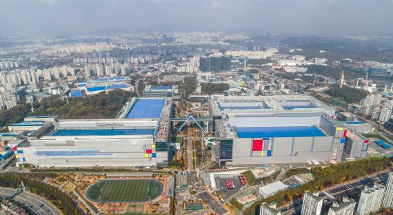
Samsung Electronics Hwaseong Campus. Courtesy of Samsung Electronics
[Financial News] It has been confirmed that Samsung Electronics has introduced the next-generation semiconductor exposure equipment, the 'High Numerical Aperture (NA) Extreme Ultraviolet (EUV) Exposure Equipment', to its Hwaseong Campus. High NA EUV is essential equipment for implementing ultra-fine circuits of 2 nanometers (1 nm = 1 billionth of a meter) or less, and this can be interpreted as Samsung Electronics' measure to increase the perfection of processes below 2 nanometers. In the future, Samsung Electronics plans to make all-out efforts to secure ultra-fine process technology and attract large customers in order to catch up with TSMC, the world's No. 1 foundry (semiconductor consignment manufacturing).
According to the semiconductor industry on the 11th, Samsung Electronics is known to have introduced 'EXE:5000', the first high NA EUV equipment produced by ASML, to its Hwaseong Campus earlier this month. The equipment in question is an expensive piece of equipment priced at 500 billion won, and ASML is the only company in the world that supplies it.
Samsung Electronics has been conducting process application evaluations for high-NA EUV equipment since last year, and it is reported that it plans to use it for next
-generation semiconductor processes below 2nm. EUV exposure equipment draws circuits in nanometer units by irradiating extreme ultraviolet rays on semiconductor wafers. The narrower the circuit line width of a semiconductor, the lower the power consumption and the faster the data processing speed. High-NA EUV equipment has further improved the performance of existing EUV equipment. High-NA is equipment that increases the NA, a numerical value indicating the light gathering ability, from 0.33 to 0.55 by increasing the size of the lens and reflector.
Accordingly, high-NA EUV is evaluated as essential equipment for next-generation foundry processes below 2nm. Global semiconductor companies are also rushing to introduce high-NA EUV. Intel is known to have signed a contract to purchase a total of six equipment, including ASML's first high-NA EUV in 2023. TSMC is also accelerating the introduction of the 2nm process by recently introducing the equipment.
There are expectations that the introduction of such equipment could be a 'reversal card' for Samsung Electronics. According to market research firm TrendForce, TSMC's foundry market share in the fourth quarter of last year was 67.1%, up 2.4 percentage points from the third and fourth quarters. On the other hand, Samsung Electronics is struggling in the market, falling 1 percentage point from 9.1% to 8.1% during the same period.
As the gap widens, there is talk that Samsung Electronics will compete in the 2nm market. It is reported that TSMC secured a 60% yield in the 2nm test production conducted at the end of last year. As Samsung Electronics also prepares to implement ultra-fine circuits this time, competition in semiconductor processes below 2nm is expected to become even fiercer. Samsung Electronics plans to complete the installation of high NA EUV equipment and begin building a full-fledged ecosystem.
It is also gearing up internally.
In his first message to executives and employees after taking office, Han Jin-man, head of Samsung Electronics' foundry business division, said, "We were the first to achieve the gate-all-around (GAA) process transition, but there are still many shortcomings in commercialization," and ordered a rapid ramp-up (increase in production capacity) of the 2nm process as the first task.

 www.fnnews.com
Intel and TSMC follow suit, essential for 2nm process
Samsung's all-out effort to seize the opportunity in the 2nm market

Samsung Electronics Hwaseong Campus. Courtesy of Samsung Electronics
[Financial News] It has been confirmed that Samsung Electronics has introduced the next-generation semiconductor exposure equipment, the 'High Numerical Aperture (NA) Extreme Ultraviolet (EUV) Exposure Equipment', to its Hwaseong Campus. High NA EUV is essential equipment for implementing ultra-fine circuits of 2 nanometers (1 nm = 1 billionth of a meter) or less, and this can be interpreted as Samsung Electronics' measure to increase the perfection of processes below 2 nanometers. In the future, Samsung Electronics plans to make all-out efforts to secure ultra-fine process technology and attract large customers in order to catch up with TSMC, the world's No. 1 foundry (semiconductor consignment manufacturing).
According to the semiconductor industry on the 11th, Samsung Electronics is known to have introduced 'EXE:5000', the first high NA EUV equipment produced by ASML, to its Hwaseong Campus earlier this month. The equipment in question is an expensive piece of equipment priced at 500 billion won, and ASML is the only company in the world that supplies it.
Samsung Electronics has been conducting process application evaluations for high-NA EUV equipment since last year, and it is reported that it plans to use it for next
-generation semiconductor processes below 2nm. EUV exposure equipment draws circuits in nanometer units by irradiating extreme ultraviolet rays on semiconductor wafers. The narrower the circuit line width of a semiconductor, the lower the power consumption and the faster the data processing speed. High-NA EUV equipment has further improved the performance of existing EUV equipment. High-NA is equipment that increases the NA, a numerical value indicating the light gathering ability, from 0.33 to 0.55 by increasing the size of the lens and reflector.
Accordingly, high-NA EUV is evaluated as essential equipment for next-generation foundry processes below 2nm. Global semiconductor companies are also rushing to introduce high-NA EUV. Intel is known to have signed a contract to purchase a total of six equipment, including ASML's first high-NA EUV in 2023. TSMC is also accelerating the introduction of the 2nm process by recently introducing the equipment.
There are expectations that the introduction of such equipment could be a 'reversal card' for Samsung Electronics. According to market research firm TrendForce, TSMC's foundry market share in the fourth quarter of last year was 67.1%, up 2.4 percentage points from the third and fourth quarters. On the other hand, Samsung Electronics is struggling in the market, falling 1 percentage point from 9.1% to 8.1% during the same period.
As the gap widens, there is talk that Samsung Electronics will compete in the 2nm market. It is reported that TSMC secured a 60% yield in the 2nm test production conducted at the end of last year. As Samsung Electronics also prepares to implement ultra-fine circuits this time, competition in semiconductor processes below 2nm is expected to become even fiercer. Samsung Electronics plans to complete the installation of high NA EUV equipment and begin building a full-fledged ecosystem.
It is also gearing up internally.
In his first message to executives and employees after taking office, Han Jin-man, head of Samsung Electronics' foundry business division, said, "We were the first to achieve the gate-all-around (GAA) process transition, but there are still many shortcomings in commercialization," and ordered a rapid ramp-up (increase in production capacity) of the 2nm process as the first task.

[단독] TSMC도 들여온 5천억 짜리 하이-NA EUV, 삼성 반입 시작 [FN 테크인사이드]
삼성전자가 차세대 반도체 노광장비인 '하이 뉴매리컬애퍼처(NA) 극자외선(EUV) 노광장비'를 화성캠퍼스에 도입한 것으로 확인됐다. 하이 NA EUV는 2나노미터(1nm=10억분의1m) 이하 초미세 회로를 구현하는데 필수적인 장비로, 삼성전자가 2나노 이하 공정 완성도..
