Array
(
    [content] => 
    [params] => Array
        (
            [0] => /forum/threads/samsung%E2%80%99s-3nm-yield-reportedly-below-20-struggling-for-mass-production.20504/
        )

    [addOns] => Array
        (
            [DL6/MLTP] => 13
            [Hampel/TimeZoneDebug] => 1000070
            [SV/ChangePostDate] => 2010200
            [SemiWiki/Newsletter] => 1000010
            [SemiWiki/WPMenu] => 1000010
            [SemiWiki/XPressExtend] => 1000010
            [ThemeHouse/XLink] => 1000970
            [ThemeHouse/XPress] => 1010570
            [XF] => 2021770
            [XFI] => 1050270
        )

    [wordpress] => /var/www/html
)

Samsung’s 3nm Yield Reportedly Below 20%, Struggling for Mass Production

fansink

Well-known member
Given Samsung has been working on 3nm for years, with extensive knowledge in this art, how does their lack of success portend Intel's similar struggles?


According to a report from Korean media outlet ZDNet Korea, the yield rate for Samsung Electronics’ latest Exynos 2500 processor has improved to slightly below 20% from single digits in the first quarter. However, the current yield rate is still said to be falling short of mass production standards. It remains uncertain whether it can be used in the flagship Galaxy S25 series smartphones in the future.
They call it 2nm now. Samsung likes to get to the party first but sometimes they are naked, but they are first. 😂
 
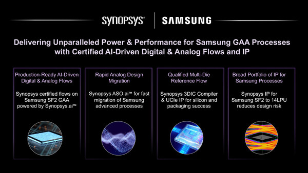
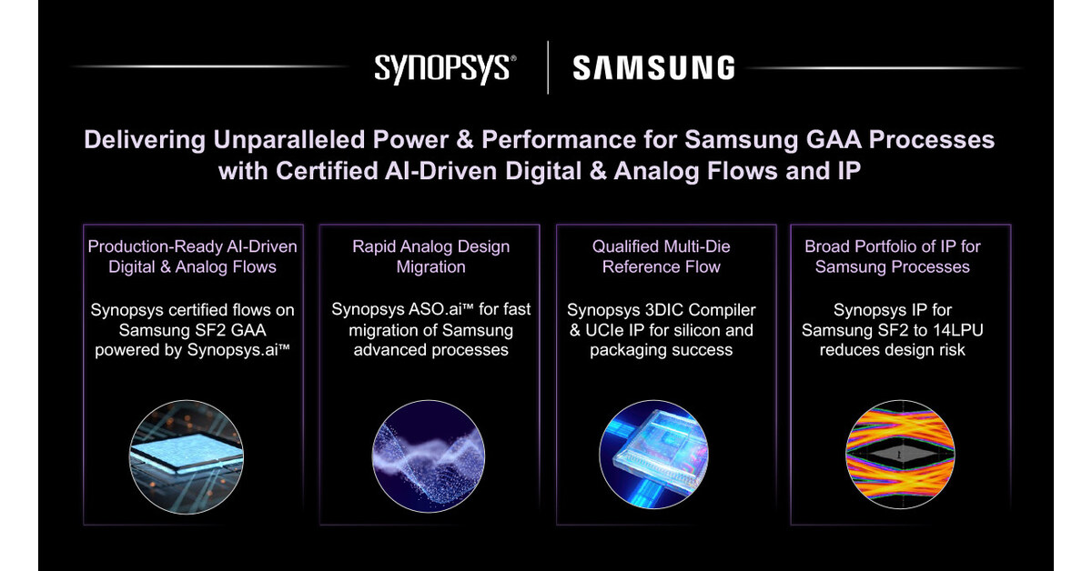
Synopsys Achieves Certification of its AI-driven Digital and Analog Flows and IP on Samsung Advanced SF2 GAA Process
Highlights

  • Synopsys_Samsung_Delivering_Unparalleled_Power_and_Performance_for_Samsung_GAA_Processes.jpg

    View File Download File
    Synopsys-Samsung-Delivering-Unparalleled-Power-and-Performance-for-Samsung-GAA-Processes
  • Silicon_Proven_Synopsys_IP_for_Samsung_Foundry.jpg

    View File Download File
    Silicon-Proven-Synopsys-IP-for-Samsung-Foundry
  • Test chip tapeouts validate product readiness of certified digital and analog design flows for Samsung Foundry SF2/SF2Z process
  • Collaboration on design techniques for SF2, including backside power and nanosheet optimization delivers more efficient power distribution
  • Synopsys IP, now available and silicon proven on Samsung SF2, reduces integration risk and accelerates silicon success
  • Qualified multi-die design reference flow and UCIe IP for SF2 process accelerates 2.5D/3D heterogeneous integration
  • Expanded collaboration on Synopsys.ai includes Synopsys ASO.ai for accelerated analog design migration with new analog design migration reference flow for Samsung's GAA processes
SUNNYVALE, Calif., June 12, 2024 /PRNewswire/ -- Synopsys, Inc. (Nasdaq: SNPS) today announced that its AI-driven digital design and analog design flows have achieved certification on Samsung Foundry's SF2 process with multiple test chip tapeouts. The reference flows, powered by the Synopsys.ai™ full-stack EDA suite, enhance PPA, boost productivity, and accelerate analog design migration for Samsung Foundry's latest Gate-All-Around (GAA) process technologies. The Samsung SF2 process was optimized using Synopsys' AI-driven design technology co-optimization (DTCO) solution which delivered significantly superior performance, power, and area (PPA) for the process compared to optimization without the use of AI. Building on this success, the same co-optimization techniques will be applied for Samsung's advanced SF1.4 process.

"The demand for custom SoCs in the era of pervasive intelligence requires extensive ecosystem collaboration to help customers accelerate their innovation and silicon success on Samsung's SF2 and next-generation SF1.4 processes," said Sanjay Bali, vice president of product management and strategy for the EDA Group at Synopsys. "Achieving certification and multiple successful tapeouts of our digital and analog flows, powered by Synopsys.ai, on the SF2 process, combined with proven Synopsys IP provides designers with a trusted path to meeting their aggressive design goals for a faster time to market."

"Synopsys and Samsung have worked closely for decades to help our mutual customers achieve their most complex design requirements," said Sangyun Kim, Vice President and head of Foundry Design Technology Team at Samsung Electronics. "This latest collaboration milestone with Synopsys on AI-driven EDA flows and broad IP portfolio development is a testament to our ongoing efforts to address the industry's growing demand for high performance computing with significant PPA gains. Working together we validated our PPA results using Synopsys' certified digital flow, achieving 12% higher performance, 25% reduction in power, and 5% area reduction compared to the base design."

Collaboration on AI-driven EDA Flows
Synopsys and Samsung are closely collaborating on AI-driven flows, including Synopsys DSO.ai™ for design productivity and PPA optimization, and Synopsys ASO.ai™ for faster analog design migration. This collaboration has resulted in a new analog design migration reference flow using Synopsys ASO.ai for Samsung's FinFET to GAA processes, enabling designers to efficiently migrate Samsung 8nm analog IPs to SF2 process, adding to Synopsys' established flows on Samsung's 14nm to 8nm/SF5 processes.

New Design Techniques and Methodology for Advanced GAA Processes
Synopsys' continued innovation helps mutual customers benefit from new design techniques including backside routing, local layout effect-aware methodology, and nanosheet cell design, to help customers meet their design goals for power, performance, and area on Samsung SF2 process family. In addition, integrating backside routing and the super-cell approach using Synopsys' digital implementation and signoff tools enables designers to increase transistor performance efficiency and density, optimize power consumption, and reduce area by up to 20% for Samsung's SF2Z process technology compared to chips without backside routing capabilities.

Accelerate SoC and Multi-Die Designs
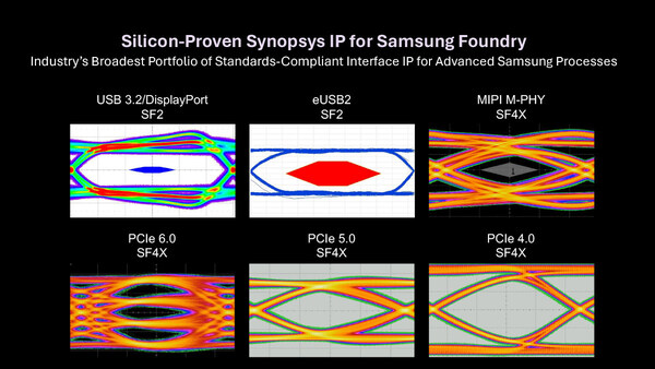
Synopsys IP for Samsung standard and automotive processes from SF2 to SF14LPU delivers a competitive edge for chipmakers looking to reduce integration risk and accelerate time to silicon success for automotive, mobile, high-performance computing (HPC) and multi-die designs. The industry's broadest portfolio of standards-compliant, silicon-proven interface IP for advanced Samsung processes, including PCIe 6.0/5.0/4.0, DDR5, LPDDR5X/5/4X, MIPI M-PHY G5, eUSB2, USB 3.2/3.1, and DisplayPort enables wide interoperability for commonly used protocols. To accelerate integration of chiplets in multi-die packages, Synopsys UCIe IP has taped out in SF2 and SF4x, and achieved silicon success in SF5A process technologies, to deliver robust die-to-die connectivity with low power and low latency. Synopsys Foundation IP, including embedded memories, logic libraries and GPIOs, is also proven in silicon to deliver leading power, performance, and area in a range of Samsung process technologies.

Mutual customers can accelerate the development of multi-die designs using Synopsys 3DIC Compiler, a unified exploration-to-signoff platform for 2.5D and 3D heterogeneous integration and advanced packaging. Qualified for Samsung Foundry's SF2 process, Synopsys 3DIC Compiler supports Samsung's advanced silicon processes, packaging technologies, and 3DCODE standard. Synopsys is an active member of the Samsung Foundries' MDI Alliance, helping mutual customers achieve a successful transition to 2.5D and 3D advanced packaging designs.

About Synopsys
Catalyzing the era of pervasive intelligence, Synopsys, Inc. (Nasdaq: SNPS) delivers trusted and comprehensive silicon to systems design solutions, from electronic design automation to silicon IP and system verification and validation. We partner closely with semiconductor and systems customers across a wide range of industries to maximize their R&D capability and productivity, powering innovation today that ignites the ingenuity of tomorrow. Learn more at www.synopsys.com.

Editorial Contact
Kelli Wheeler
Synopsys, Inc.
(650) 584-5000
kelliw@synopsys.com
corp-pr@synopsys.com


SOURCE Synopsys, Inc.
 
Sounds like a rinse and repeat of prior nodes. Yeah advanced node is really hard but Koreans aren’t dumb, you’d think with the same tools and resources they’d figure it out, something really broken there
 
Given Samsung has been working on 3nm for years, with extensive knowledge in this art, how does their lack of success portend Intel's similar struggles?
Best case for Samsung it is just as bad, but I think there is a strong case that it is worse than it ever was with intel. i14nm was 6-9 mo late, i10nm was 2-3 years late (depending on if you want to go with the 2016 date or the 2017 date for HVM), and i7nm was 1 year late.

Samsung 10LPE was atrocious and early 10LPP was also really bad. I remember Nvidia talking about 8LPP having worse than expected yields hurting their client Ampere volume. 7LPP was a year late (even if Samsung pretends it wasn't). Albeit this seems to been from EUV productivity rather than early yield, but no way to know for sure. 6LPE was vaporware. 5LPE had poor parametrics, yields, and PPA; while also being later than N5. 4LPE was low yield and while the area problem was solved, P&P was closer to 7"nm" class than 5"nm" class. 4LPP/SF4 seems to be like 1-2 years late, and SF4/4P still don't seem to be competitive with even N5P P&P. 3GAE entered """"HVM""""' in 2022, and 3GAP/SF3 was supposed to enter HVM in 2023.

Considering 3GAE's only product to date was an ultra low volume 20mm^2 bitcoin ASIC (high on-die redundancy and basically no performance requirement), with no SRAM, no analog, nor DRAM PHY, and no inner spacer (huge power and performance hit to doing that) I would say they will be at least 2 years late if no commercially available GAA product ships this year. If this rumor is true and 2025's Exynos 2500 is canned or sees some cannon lake like paper launch like the first 4LPE SOCs did, then Samsung 3nm is as bad or worse than intel 10nm and this would be off an even longer trail of dud processes than intel had.
Something is deeply broken systemically at Samsung foundry
Agreed. While I know many would roll their eyes at the following comment; but I am willing to give them a bit more time. A lot of leadership got changed recently, process node R&D has a long horizon, and changing culture is a slow process. I think new leadership has until SF1.4 to show if they are on a path to recovery. Ann Kelleher got put in charge of the newly liberated TD group in mid 2020 and proof points of intel recovery only started materializing in 2023/24. SF1.4 is far enough out that changes can be made to how Samsung develops process technology and culture can start to shift, and I think the new team deserves ONE instance of benefit of the doubt.
 
Best case for Samsung it is just as bad, but I think there is a strong case that it is worse than it ever was with intel. i14nm was 6-9 mo late, i10nm was 2-3 years late (depending on if you want to go with the 2016 date or the 2017 date for HVM), and i7nm was 1 year late.

Samsung 10LPE was atrocious and early 10LPP was also really bad. I remember Nvidia talking about 8LPP having worse than expected yields hurting their client Ampere volume. 7LPP was a year late (even if Samsung pretends it wasn't). Albeit this seems to been from EUV productivity rather than early yield, but no way to know for sure. 6LPE was vaporware. 5LPE had poor parametrics, yields, and PPA; while also being later than N5. 4LPE was low yield and while the area problem was solved, P&P was closer to 7"nm" class than 5"nm" class. 4LPP/SF4 seems to be like 1-2 years late, and SF4/4P still don't seem to be competitive with even N5P P&P. 3GAE entered """"HVM""""' in 2022, and 3GAP/SF3 was supposed to enter HVM in 2023.

Considering 3GAE's only product to date was an ultra low volume 20mm^2 bitcoin ASIC (high on-die redundancy and basically no performance requirement), with no SRAM, no analog, nor DRAM PHY, and no inner spacer (huge power and performance hit to doing that) I would say they will be at least 2 years late if no commercially available GAA product ships this year. If this rumor is true and 2025's Exynos 2500 is canned or sees some cannon lake like paper launch like the first 4LPE SOCs did, then Samsung 3nm is as bad or worse than intel 10nm and this would be off an even longer trail of dud processes than intel had.

Agreed. While I know many would roll their eyes at the following comment; but I am willing to give them a bit more time. A lot of leadership got changed recently, process node R&D has a long horizon, and changing culture is a slow process. I think new leadership has until SF1.4 to show if they are on a path to recovery. Ann Kelleher got put in charge of the newly liberated TD group in mid 2020 and proof points of intel recovery only started materializing in 2023/24. SF1.4 is far enough out that changes can be made to how Samsung develops process technology and culture can start to shift, and I think the new team deserves ONE instance of benefit of the doubt.

Thanks @nghanayem, that is a lot of useful information to digest, I may need a decoder ring 🤔
 
Best case for Samsung it is just as bad, but I think there is a strong case that it is worse than it ever was with intel. i14nm was 6-9 mo late, i10nm was 2-3 years late (depending on if you want to go with the 2016 date or the 2017 date for HVM), and i7nm was 1 year late.

Samsung 10LPE was atrocious and early 10LPP was also really bad. I remember Nvidia talking about 8LPP having worse than expected yields hurting their client Ampere volume. 7LPP was a year late (even if Samsung pretends it wasn't). Albeit this seems to been from EUV productivity rather than early yield, but no way to know for sure. 6LPE was vaporware. 5LPE had poor parametrics, yields, and PPA; while also being later than N5. 4LPE was low yield and while the area problem was solved, P&P was closer to 7"nm" class than 5"nm" class. 4LPP/SF4 seems to be like 1-2 years late, and SF4/4P still don't seem to be competitive with even N5P P&P. 3GAE entered """"HVM""""' in 2022, and 3GAP/SF3 was supposed to enter HVM in 2023.

Considering 3GAE's only product to date was an ultra low volume 20mm^2 bitcoin ASIC (high on-die redundancy and basically no performance requirement), with no SRAM, no analog, nor DRAM PHY, and no inner spacer (huge power and performance hit to doing that) I would say they will be at least 2 years late if no commercially available GAA product ships this year. If this rumor is true and 2025's Exynos 2500 is canned or sees some cannon lake like paper launch like the first 4LPE SOCs did, then Samsung 3nm is as bad or worse than intel 10nm and this would be off an even longer trail of dud processes than intel had.

Agreed. While I know many would roll their eyes at the following comment; but I am willing to give them a bit more time. A lot of leadership got changed recently, process node R&D has a long horizon, and changing culture is a slow process. I think new leadership has until SF1.4 to show if they are on a path to recovery. Ann Kelleher got put in charge of the newly liberated TD group in mid 2020 and proof points of intel recovery only started materializing in 2023/24. SF1.4 is far enough out that changes can be made to how Samsung develops process technology and culture can start to shift, and I think the new team deserves ONE instance of benefit of the doubt.
Agreed. They deserve a couple more swings of the bat certainly. Still just shocking how leadership let things derail so spectacularly.
 
TSMC is manufacturing the newest and most advanced smartphone SoCs from MediaTek and Qualcomm that Samsung smartphones use. It means Samsung's revenue and profit are tightly depending on TSMC's yield, cost, quality, and performance. Turn around Samsung smartphone sales affects TSMC's revenue and profit too. It's really a small world.

Samsung smartphone division generated $24 billion sales out of $52.6 billion Samsung's Q1 2024 revenue.

 
Last edited:
Given Samsung has been working on 3nm for years, with extensive knowledge in this art, how does their lack of success portend Intel's similar struggles?
Feels like a huge opportunity for Intel.. If Intel can demonstrate real volume of 18A in the next 18 months then they’ll be set to take a lot of business over time from Samsung.
 
Feels like a huge opportunity for Intel.. If Intel can demonstrate real volume of 18A in the next 18 months then they’ll be set to take a lot of business over time from Samsung.

That seems unlikely, given their 3nm is ~not yielding higher than Samsung's, else I suspect Gelsinger would be yodeling such from the mountaintops.

Pat would at least be bragging about having surpassed Samsung's 3nm, without mentioning yields.
 
That seems unlikely, given their 3nm is ~not yielding higher than Samsung's, else I suspect Gelsinger would be yodeling such from the mountaintops.

Pat would at least be bragging about having surpassed Samsung's 3nm, without mentioning yields.
Maybe - you don't usually shout "we are #2!!" When you are aiming to be #1.

We will know how Intels 3 yields are soon. They have sampled a lot of large die server chips already based on 3.
 
Maybe - you don't usually shout "we are #2!!" When you are aiming to be #1.

We will know how Intels 3 yields are soon. They have sampled a lot of large die server chips already based on 3.

Pat can't pass any opportunity to brag, especially in the tenuous position he's in

Samples are no indication of yield, since they are binned at very low frequency if necessary (like best die out of 50 wafers)
 
Pat can't pass any opportunity to brag, especially in the tenuous position he's in

Samples are no indication of yield, since they are binned at very low frequency if necessary (like best die out of 50 wafers)
Like I said we will see in a few months..

I don't know off hand if Intel 3 and Samsung 3GAE are in the same league for density or performance, but all indications are Intel is on track for yielding chips that are much larger than what Samsung is producing at "3nm".
 
Best case for Samsung it is just as bad, but I think there is a strong case that it is worse than it ever was with intel. i14nm was 6-9 mo late, i10nm was 2-3 years late (depending on if you want to go with the 2016 date or the 2017 date for HVM), and i7nm was 1 year late.

Samsung 10LPE was atrocious and early 10LPP was also really bad. I remember Nvidia talking about 8LPP having worse than expected yields hurting their client Ampere volume. 7LPP was a year late (even if Samsung pretends it wasn't). Albeit this seems to been from EUV productivity rather than early yield, but no way to know for sure. 6LPE was vaporware. 5LPE had poor parametrics, yields, and PPA; while also being later than N5. 4LPE was low yield and while the area problem was solved, P&P was closer to 7"nm" class than 5"nm" class. 4LPP/SF4 seems to be like 1-2 years late, and SF4/4P still don't seem to be competitive with even N5P P&P. 3GAE entered """"HVM""""' in 2022, and 3GAP/SF3 was supposed to enter HVM in 2023.

Considering 3GAE's only product to date was an ultra low volume 20mm^2 bitcoin ASIC (high on-die redundancy and basically no performance requirement), with no SRAM, no analog, nor DRAM PHY, and no inner spacer (huge power and performance hit to doing that) I would say they will be at least 2 years late if no commercially available GAA product ships this year. If this rumor is true and 2025's Exynos 2500 is canned or sees some cannon lake like paper launch like the first 4LPE SOCs did, then Samsung 3nm is as bad or worse than intel 10nm and this would be off an even longer trail of dud processes than intel had.

Agreed. While I know many would roll their eyes at the following comment; but I am willing to give them a bit more time. A lot of leadership got changed recently, process node R&D has a long horizon, and changing culture is a slow process. I think new leadership has until SF1.4 to show if they are on a path to recovery. Ann Kelleher got put in charge of the newly liberated TD group in mid 2020 and proof points of intel recovery only started materializing in 2023/24. SF1.4 is far enough out that changes can be made to how Samsung develops process technology and culture can start to shift, and I think the new team deserves ONE instance of benefit of the doubt.
If my memory is correct, Sanjay Natarajan was recruited back from AMAT to lead TD for 20A/18A with Ann Kelleher. Sanjay seems not on the role now. What was his contribution?
 
Back
Top