В России написана «дорожная карта» создания суверенного литографа дешевле и проще, чем у ASML - CNews
В России разработан план создания оборудования для создания современных чипов, которое будет дешевле и эффективнее...
Russia has written a “road map” for creating a sovereign lithograph cheaper and simpler than ASML
Russia has developed a plan to create equipment for creating modern chips, which will be cheaper and more efficient than the installations of today's market monopolist ASML. The authors of the project believe that it is inappropriate for our country to follow the path of the Dutch company, since it is too expensive. Therefore, Russia will create installations not with a wavelength of 13.5, but 11.2 nanometers.
"Roadmap" for the creation of a Russian lithograph
Russia has developed a "road map" for creating a lithograph that will be cheaper and easier to manufacture than the equipment of the Dutch ASML. But at the same time, the Russian installation will be no less effective. This follows from the "New concept for the development of high-performance X-ray lithography" prepared by Nikolai Chkhalo , an employee of the Institute of Physics of Microstructures of the Russian Academy of Sciences (IPM RAS) , which was obtained by CNews.
The implementation of the “road map” will allow the country to create its own modern nanolithographic installations within a reasonable time frame, the document notes.
IPM RAS proposes to reduce the operating wavelength of the lithograph from 13.5 to 11.2 nm. It is expected that this approach will reduce the costs of both the production of vacuum elements and systems, and the lithograph as a whole, as well as the cost of operation.
Innovative concept
To create a domestic lithograph that is not inferior to ASML , IPM RAS offers a number of innovations. For example, a wavelength of 11.2 nm. This should lead to an increase in the resolution of the installation by 20% (resolution is defined as the minimum element reproduced in the photoresist layer).
"This will reduce the overall dimensions and significantly simplify the manufacture of mirrors, as well as significantly reduce the cost of lens production ," notes Chkhalo. "In the Russian installation, it is planned to replace the tin laser- plasma source with a xenon one. This should significantly reduce contamination of optical elements with the spread products of the source material. The service life of the expensive collector and pellicle (free-hanging multilayer films for protecting masks), and therefore the masks, will increase several times."
The transition to a wavelength of 11.2 nm potentially opens up the possibility of using silicon-based resists, in particular organosilicon ones. Organic resists have the highest sensitivity at high pattern transfer parameters in EUV lithography, follows from the concept. "It can be expected that an increase in the proportion of silicon in the resist will lead to a noticeable increase in the efficiency of the resist at a wavelength of 11.2 nm compared to 13.5 nm," Chkhalo emphasizes.
Comparison of Russian and ASML lithograph
The table provides a comparison of the main parameters of the TWINSCAN NXE:3600D lithograph manufactured by ASML with the expected parameters of the lithograph being developed at the IPM RAS .
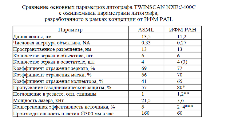
Comparison of the characteristics of the future Russian lithograph and the existing ASML lithograph from the "Concept for the development of high-performance X-ray lithography"
As can be seen from the table, with an average laser power of 3.6 kW, the expected productivity at a wavelength of 11.2 nm will be approximately 2.7 times less than that of the ASML lithograph.
“For factories whose product market is smaller than that of the top 5 companies, this value is quite sufficient, given that of all the layers on the chip, X-ray lithography is used only when forming several critical layers,” the document notes. “Thus, successful implementation of this concept will allow achieving the goals of increasing the availability of X-ray lithography for users without compromising resolution.”
Work in three stages
By analogy with the experience of developing global EUV lithography, the implementation of the proposed concept involves three stages, Chkhalo cites.
The first stage consists of research and development work (R&D) with elements of experimental design work ( EDW ). It is planned to create critical technologies of X-ray lithography, identify the main problems in all key technologies and develop proposals for correcting technical solutions.
In addition, it is planned to form cooperation links and a list of equipment necessary to solve the tasks of the second stage. To create an experimental sample of a lithograph for testing all elements in a real technological process, to develop resists and to work out technologies for forming nanostructures using the X-ray lithography method.
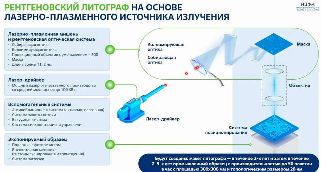
The NCFM is also involved in the development of a lithograph with a wavelength of 11.2 nm (frame from the NCFM presentation)
The goals of the second stage include the creation of a prototype of a high-performance lithograph with a six-mirror projection lens, a multi-kilowatt laser system, and a scanning system for 200/300 mm plates. In particular, it is planned to integrate X-ray lithography into the high-performance line of production of advanced domestic chips, and to create cooperation chains for the production of the main elements and systems of the lithograph.
The results of this stage will be a prototype lithograph with a capacity of over 60 200 mm plates per hour. It is also planned to integrate X-ray lithography into the technological chain of chip production at an advanced domestic factory, allowing this technology to be used in the production of critical layers with minimal topological standards, as well as the formulation of technical specifications and a feasibility study for a prototype lithograph for industrial applications.
The third stage involves the creation of a lithograph adapted for use at a factory, with a productivity of more than 60 plates with a diameter of 300 mm per hour, and the organization of serial production of lithographs in Russia.
The timeframes for completing the stages are not specified in the document.
CNews reported on the start of work on the lithograph at the IAP RAS in October 2022. It was assumed that the installation would be able to produce chips using a 7 nm topology. The equipment may begin full operation in 2028. The RAS expects that the Russian lithograph will be 1.5-2 times more efficient than the one created by ASML.
ASML Experience
Chkhalo is convinced that trying to copy ASML's lithograph will not succeed. This conclusion applies to both the technical and economic problems that stand in the way of building a 13.5 nm lithograph, he continues.
“In general, the concept developed by ASML has led to huge equipment costs,” notes Chkhalo. “According to various sources, the price of the currently manufactured NXE:3400C and NXE:3600D series lithographs exceeds 300 million euros, and the new generation EXE:5000 with a resolution of 8 nm is several times higher.”
Nevertheless, top managers of TSMC, Samsung and Intel confirm that, despite all these costs, EUV lithography is cost-effective, the document notes. "However, it should be taken into account that this efficiency is due to the gigantic chip market occupied by these companies, essentially monopolists ," it goes on. "With a reduction in the market, this efficiency will fall sharply. Indirect confirmation of this conclusion is the fact that, apart from these giants, as well as the American Micron Technology and the Korean SK Hynix Korea, which are among the top 5 chip manufacturers in the world, no one else has purchased such equipment and, according to ASML forecasts, no one plans to do so in the near future."
Therefore, Chkhalo comes to the conclusion that from an economic point of view, repeating the ASML project for Russia is pointless. Since in small-scale production it may exceed the cost of the special equipment for which this chip was produced.
Technically, it seems unlikely that ASML's development will be repeated, and the use of such equipment for the domestic chip market with its limited volume does not seem advisable.
The incredible technological difficulties of creating an EUV lithograph meant that even the US and Japan , having started this race first, were unable to bring their EUV programs to a competitive product and were limited to just individual components for ASML.
"The reason for their failure, and, in contrast, ASML's success, in our opinion, is that ASML was able to integrate the best world achievements in all major components into its product," Chkhalo continues. "They achieved this through unprecedented openness of the project. Based on this, we can conclude that in a technological sense, it is unlikely that one country will repeat the ASML project."
Therefore, it is obvious to the author that the domestic program requires an alternative approach to solving the problem of high-performance X-ray lithography, providing comparable technical characteristics and at the same time making this technology more affordable in terms of equipment price and operating costs. If this concept is implemented, lithographs will be in demand not only in the Russian Federation, but also abroad, as they will become available to companies that are not in the top 5.
Lithography in Russia
Let us recall that due to sanctions , lithography equipment is not imported into Russia. So, domestic production is an important step towards technological sovereignty.
The production of Russian equipment for the production of chips with a 350 nm topology will begin in 2024, and 130 nm - in 2026. Such ambitious plans were voiced by Deputy Minister of Industry and Trade Vasily Shpak . Today, only two companies in the world produce such lithography - the Dutch ASML and the Japanese Nikon .
After 2026, Russia will begin a relatively large-scale production of lithography lasers, which will be used to produce microcircuits. It is planned to assemble at least five such lasers per year. Development is in full swing: test trials as part of a lithograph are scheduled for 2025.
The laser was developed by the Lassard Group . The testing will be carried out by employees of the Zelenograd Nanotechnology Center ( ZNTS ), and the laser itself will be used as part of a lithograph, initially designed for a 350 nm topology. The new laser will "pump up" it to 130 nm. For comparison, the most modern technological process, by which various microcircuits are manufactured in 2024, including central processors , is 3 nm. These standards are used at TSMC factories to manufacture Apple chips .
In its original design, it is intended for the production of chips using a 350 nm topology. This is not the most modern technological process - the peak of its relevance came in 1995-1996. Although 350 nanometer chips are considered large-sized chips , they are still used in many industries, including the automotive industry, energy and telecommunications.
CNews wrote about the problems associated with the implementation of such projects. First, budgets . The authorities will spend 100 billion rubles to build an industry in Russia to produce equipment for the production of microcircuits. The money will be allocated over three years. For comparison, in 2022 alone, ASML, the largest vendor of such equipment in the world, invested three times more money in R&D . In addition, there are almost no needed specialists in Russia , and those who were found are already about 80 years old.
“Companies do not have enough employees capable of calculating the technological process of such installations, nor scientists with sufficient knowledge in the field of, for example, practical physics ,” noted Evgeny Gornev, Deputy Head of the Department of Micro- and Nanoelectronics at MIPT .