Market rumors suggest that Nvidia will manufacture its own HBM Base Die, shaking up the HBM ecosystem. (Photo/File photo of this newspaper)

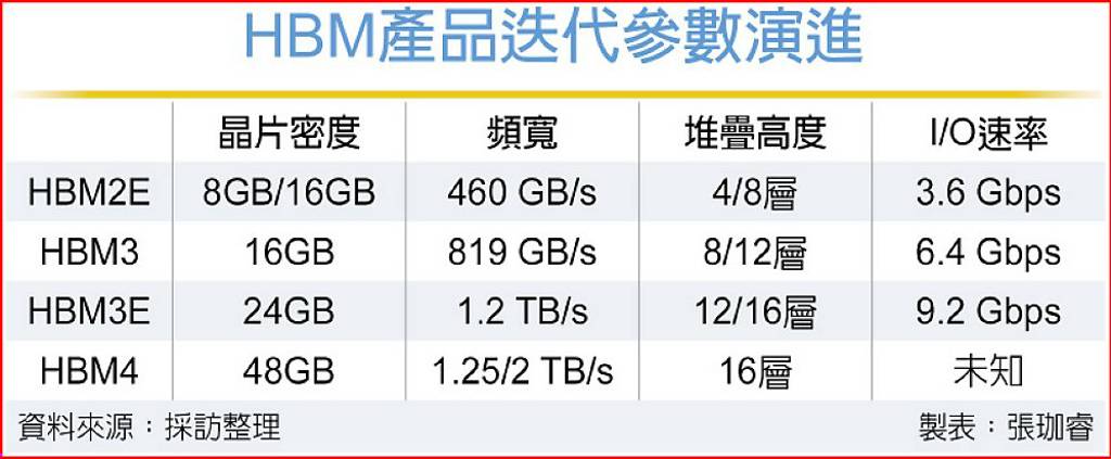
HBM product iteration parameter evolution
Market rumors have it that NVIDIA has launched its own HBM (High Bandwidth Memory) Base Die design plan. In the future, regardless of which memory brand's HBM stacked products are used, the underlying logic die (Base Die) will adopt NVIDIA's own design solution, with the process node locked at 3nm. It is estimated that small-scale trial production will begin in the second half of 2027.
This news shocked the HBM ecosystem, and market insiders worried that it might rewrite the next generation HBM market competition landscape.
SK Hynix currently holds the largest HBM market share, and its HBM base dies are primarily manufactured in-house. However, industry experts point out that increasing HBM transmission speeds to 10Gbps or higher requires the use of TSMC's advanced logic processes, such as 12nm or higher, to manufacture the base dies. Standard HBM4 can be supported using TSMC's 12nm process, and SK Hynix maintains control of the relevant supply chain.
However, memory manufacturers are relatively weak in complex base die IP and ASIC design capabilities. IC design experts point out that if HBM4 needs to integrate the UCIe high-speed interface for external communication with GPUs and CPUs, the base die design complexity will increase significantly. ASIC companies such as Creative already have complete IP and design platforms and can provide them to cloud service providers (CSPs).
Industry analysts believe that Nvidia plans to manufacture its own HBM Base Die, targeting the ASIC market with the intention of providing customers with more modular options on its NVLink Fusion open architecture platform and strengthening its control over the ecosystem.
However, outsiders believe that CSP manufacturers initially invested in ASICs precisely because they did not want to be constrained by Nvidia. Therefore, they may not be willing to adopt Nvidia's HBM Base Die. Preliminary assessments show that the actual impact on ASIC manufacturers is limited.
On the other hand, SK Hynix, the leader in HBM technology, announced earlier that it would provide new-generation 12-layer stacked HBM4 samples to major customers. Combined with advanced MR-MUF packaging technology, the capacity can reach 36GB and the bandwidth exceeds 2TB per second, which is more than 60% higher than the previous generation HBM3E bandwidth, demonstrating its leadership in the AI memory market.
SK Hynix also revealed that it will introduce the logic process of the world's leading wafer foundry in HBM Base Die in the future to continuously improve product performance and energy efficiency.
Overall, the HBM4 generation will usher in a new era of higher speeds, higher stacking, and more complex packaging integration. With Nvidia planning to manufacture its own base die and SK Hynix accelerating HBM4 mass production, the HBM market is entering a new wave of competition and change.
