I've been wondering if somebody ever attempted to make monolithic SRAM like flash people did VNAND.
To my surprise, it was very few. While 6T SRAM cell is much more complex than a single flash cell, and rows also need sense amps for fast operation, it's still comparable by number of materials, and steps needed.
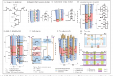
I came upon the thing below while looking for existing designs
 . A structure with a lot of vertical metal connections, and repetitive layers of individually grown nanowire FETs. The layering of p, and n doped silicon was the only easy thing about it.

At first, I was confused, am I looking on it in the right orientation? Then it hit me that I did!
The first thing I though after was "what if we turn it on its SIDE?" Like in a V-NAND.

That way bitlines, and VDD become just metal layers, which should be much easier to deal with if you can somehow access them from the side, which I believe is doable as in staircase 3D flash. Though, you will have to deal with depositing new silicon layers above metal.
A gate (CG) also becomes a layer!
Multiple isolation oxide layers (HI on the diagram) would turn into a single deposition into RIE cut trenches, like STI.
Even more importantly, you can do away with repetitively grown nanowire channel layers by replacing horizontal nanowires with RIE punch through all layers, and a single deposition for channels.

One downside of the design would be abandoning p, and n doping layers, and having to somehow do it horizontally. I believe the it should not be a problem with low layer count with simple ion implantation. A second option, you can deposit layers of intrinsic, carve deep trenches in it, and then somehow p, and n dope it horizontally after building up layers.
As a bonus from p, and n doping going in horizontal dimension, you can zigzag, and stagger doping regions if you look from the top. That should help a bit with leakage, and reduce the length of metal in between SRAM cell parts.
Last question, is where to put sense amps? Naturally, the first what comes to mind is on the side, where bitlines would stick out. Those bitlines would be quite long, and probably have much higher capacitance than 2D sram ones. One should find a way to get them as close to bitline ending as possible.
What do you people think?
To my surprise, it was very few. While 6T SRAM cell is much more complex than a single flash cell, and rows also need sense amps for fast operation, it's still comparable by number of materials, and steps needed.
I came upon the thing below while looking for existing designs
Ultra high density 3D SRAM cell design in Stacked Horizontal Nanowire (SN3D) fabric
CMOS scaling faces numerous challenges, among which device scaling, interconnect bottleneck, high leakage power and manufacturability are major ones. The scaling challenge is particularly acute for SRAM since maximum performance/power at highest density is required with every new generation. 3-D...
ieeexplore.ieee.org
At first, I was confused, am I looking on it in the right orientation? Then it hit me that I did!
The first thing I though after was "what if we turn it on its SIDE?" Like in a V-NAND.
That way bitlines, and VDD become just metal layers, which should be much easier to deal with if you can somehow access them from the side, which I believe is doable as in staircase 3D flash. Though, you will have to deal with depositing new silicon layers above metal.
A gate (CG) also becomes a layer!
Multiple isolation oxide layers (HI on the diagram) would turn into a single deposition into RIE cut trenches, like STI.
Even more importantly, you can do away with repetitively grown nanowire channel layers by replacing horizontal nanowires with RIE punch through all layers, and a single deposition for channels.
One downside of the design would be abandoning p, and n doping layers, and having to somehow do it horizontally. I believe the it should not be a problem with low layer count with simple ion implantation. A second option, you can deposit layers of intrinsic, carve deep trenches in it, and then somehow p, and n dope it horizontally after building up layers.
As a bonus from p, and n doping going in horizontal dimension, you can zigzag, and stagger doping regions if you look from the top. That should help a bit with leakage, and reduce the length of metal in between SRAM cell parts.
Last question, is where to put sense amps? Naturally, the first what comes to mind is on the side, where bitlines would stick out. Those bitlines would be quite long, and probably have much higher capacitance than 2D sram ones. One should find a way to get them as close to bitline ending as possible.
What do you people think?
Attachments
Last edited: