Source:
Intel targets more than 10x density improvement in packaging and 30% to 50% logic scaling improvements, and looks beyond classic silicon transistors.
")
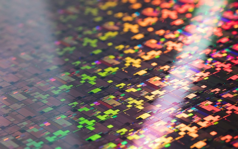
Components Research, the research group of Intel Technology Development, is responsible for delivering revolutionary process and packaging technology options that extend Moore’s Law and enable Intel products and services. (Credit: Intel Corporation)
December 11, 2021 04:30 PM Eastern Standard Time
SANTA CLARA, Calif.--(
BUSINESS WIRE)--
What’s New: In its relentless pursuit of Moore’s Law, Intel is unveiling key packaging, transistor and quantum physics breakthroughs fundamental to advancing and accelerating computing well into the next decade. At
IEEE International Electron Devices Meeting (IEDM) 2021, Intel outlined its path toward more than 10x interconnect density improvement in packaging with hybrid bonding, 30% to 50% area improvement in transistor scaling, major breakthroughs in new power and memory technologies, and new concepts in physics that may one day revolutionize computing.
“At Intel, the research and innovation necessary for advancing Moore’s Law never stops. Our Components Research Group is sharing key research breakthroughs at IEDM 2021 in bringing revolutionary process and packaging technologies to meet the insatiable demand for powerful computing that our industry and society depend on. This is the result of our best scientists’ and engineers’ tireless work. They continue to be at the forefront of innovations for continuing Moore’s Law.”
–Robert Chau, Intel Senior Fellow and general manager of Components Research
Why It Matters: Moore’s Law has been tracking innovations in computing that meet the demands of every technology generation from mainframes to mobile phones. This evolution is continuing today as we move into a new era of computing with unlimited data and artificial intelligence.
Continuous innovation is the cornerstone of Moore’s Law. Intel’s Components Research Group is committed to innovating across three key areas: essential scaling technologies for delivering more transistors; new silicon capabilities for power and memory gains; and exploration of new concepts in physics to revolutionize the way the world does computing. Many of the innovations that broke through previous barriers of Moore’s Law and are in today’s products started with the work of Component Research – including strained silicon, Hi-K metal gates, FinFET transistors, RibbonFET, and packaging innovations including EMIB and Foveros Direct.
How We Are Doing It: The breakthroughs revealed at IEDM 2021 demonstrate Intel is on track to continue the advancement and benefits of Moore’s Law well beyond 2025 through its three areas of pathfinding.
1. Intel is pursuing significant research in essential scaling technologies for delivering more transistors in future product offerings:
- Researchers at the company have outlined solutions for the design, process, and assembly challenges of hybrid bonding interconnect, envisioning a more than 10x interconnect density improvement in packaging. At the Intel Accelerated event in July, Intel announced plans to introduce Foveros Direct, enabling sub-10-micron bump pitches, providing an order of magnitude increase in the interconnect density for 3D stacking. To enable the ecosystem to gain benefits of advanced packaging, Intel is also calling for the establishment of new industry standards and testing procedures to enable a hybrid bonding chiplet ecosystem.
- Looking beyond its gate-all-around RibbonFET, Intel is mastering the coming post-FinFET era with an approach to stacking multiple (CMOS) transistors that aims to achieve a maximized 30% to 50% logic scaling improvement for the continued advancement of Moore’s Law by fitting more transistors per square millimeter.
- Intel is also paving the way for Moore’s Law advancement into the angstrom era with forward-looking research showing how novel materials just a few atoms thick can be used to make transistors that overcome the limitations of conventional silicon channels, enabling millions more transistors per die area for evermore powerful computing in the next decade.
2. Intel is bringing new capabilities to silicon:
- More efficient power technologies are advancing through the world’s first integration of GaN-based power switches with silicon-based CMOS on a 300 mm wafer. This sets the stage for low-loss, high-speed power delivery to CPUs while simultaneously reducing motherboard components and space.
- Another advancement is Intel’s industry-leading, low-latency read/write capabilities using novel ferroelectric materials for possible next-generation embedded DRAM technology that can deliver greater memory resources to address the growing complexity of compute applications, from gaming to AI.
3. Intel is pursuing massive performance with silicon transistor-based quantum computing, as well as entirely new switches for massively energy-efficient computing with novel room temperature devices. In the future, these revelations may replace classic MOSFET transistors by using entirely new concepts in physics:
- At IEDM 2021, Intel demonstrated the world’s first experimental realization of a magnetoelectric spin-orbit (MESO) logic device at room temperature, which showed the potential manufacturability for a new type of transistor based on switching nanoscale magnets.
- Intel and IMEC are making progress with spintronic materials research to take device integration research close to realizing a fully functional spin-torque device.
- Intel also showcased full 300 mm qubit process flows for the realization of scalable quantum computing that is compatible with CMOS manufacturing and identifies next steps for future research.
About Components Research: Components Research, the research group of Intel Technology Development, is responsible for delivering revolutionary process and packaging technology options that extend Moore’s Law and enable Intel products and services. It keeps Intel’s research and development pipeline full by working with the company’s business units to anticipate future needs and collaborating with external groups – from U.S. government research labs and industry consortia to university research groups and suppliers.
More Context: 3D Stacked Transistors: Improving Area by Building Upward (Video) |
Foveros Direct: Advanced Packaging Technology to Continue Moore’s Law (Video) |
Intel's Components Research Group Invents Revolutionary Process and Package Tech (Video)
About Intel
Intel (Nasdaq: INTC) is an industry leader, creating world-changing technology that enables global progress and enriches lives. Inspired by Moore’s Law, we continuously work to advance the design and manufacturing of semiconductors to help address our customers’ greatest challenges. By embedding intelligence in the cloud, network, edge and every kind of computing device, we unleash the potential of data to transform business and society for the better. To learn more about Intel’s innovations, go to
newsroom.intel.com and
intel.com.
Legal Notices
All product and service plans and roadmaps are subject to change without notice. Any forecasts of goods and services needed for Intel's operations are provided for discussion purposes only. Intel will have no liability to make any purchase in connection with forecasts published in this document. Code names are often used by Intel to identify products, technologies, or services that are in development and usage may change over time. No license (express or implied, by estoppel or otherwise) to any intellectual property rights is granted by this document. Product and process performance varies by use, configuration and other factors. Learn more at
www.Intel.com/PerformanceIndex and
www.Intel.com/ProcessInnovation.
Reference to research results, including comparisons to technologies, products, process or package performance are estimates and do not imply availability. Release dates and/or capabilities referenced may vary by use, configuration and other factors. The products and services described may contain defects or errors which may cause deviation from published specifications. Current characterized errata are available on request. Intel disclaims all express and implied warranties, including without limitation, the implied warranties of merchantability, fitness for a particular purpose, and non-infringement, as well as any warranty arising from course of performance, course of dealing, or usage in trade.
Statements in this document that refer to future plans or expectations are forward-looking statements. These statements are based on current expectations and involve many risks and uncertainties that could cause actual results to differ materially from those expressed or implied in such statements. For more information on the factors that could cause actual results to differ materially, see our most recent earnings release and SEC filings at
www.intc.com.
© Intel Corporation. Intel, the Intel logo and other Intel marks are trademarks of Intel Corporation or its subsidiaries. Other names and brands may be claimed as the property of others.
Contacts
Bruce Fienberg
1-510-220-6461
bruce.fienberg@intel.com

 www.reuters.com

")