Intel Foundry has received and assembled the industry’s first High Numerical Aperture (High NA) Extreme Ultraviolet (EUV) lithography system. The new tool provides the ability to dramatically improve resolution and feature scaling for the next generation of processors, enabling Intel Foundry to continue process leadership beyond Intel 18A.
High NA EUV is the next-generation lithography system developed by ASML following decades of collaboration with Intel. As the first mover on High NA EUV, Intel Foundry will be able to deliver never-before-seen precision and scalability in chip manufacturing. This in turn will allow Intel to develop chips with the most innovative features and capabilities – processors that are essential for driving advancements in AI and other emerging technologies.
News

Download full infographic
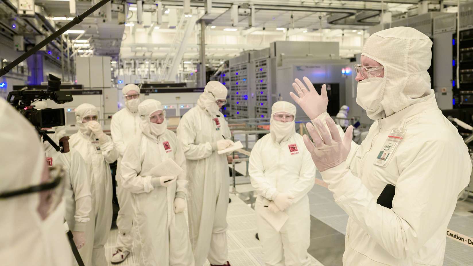
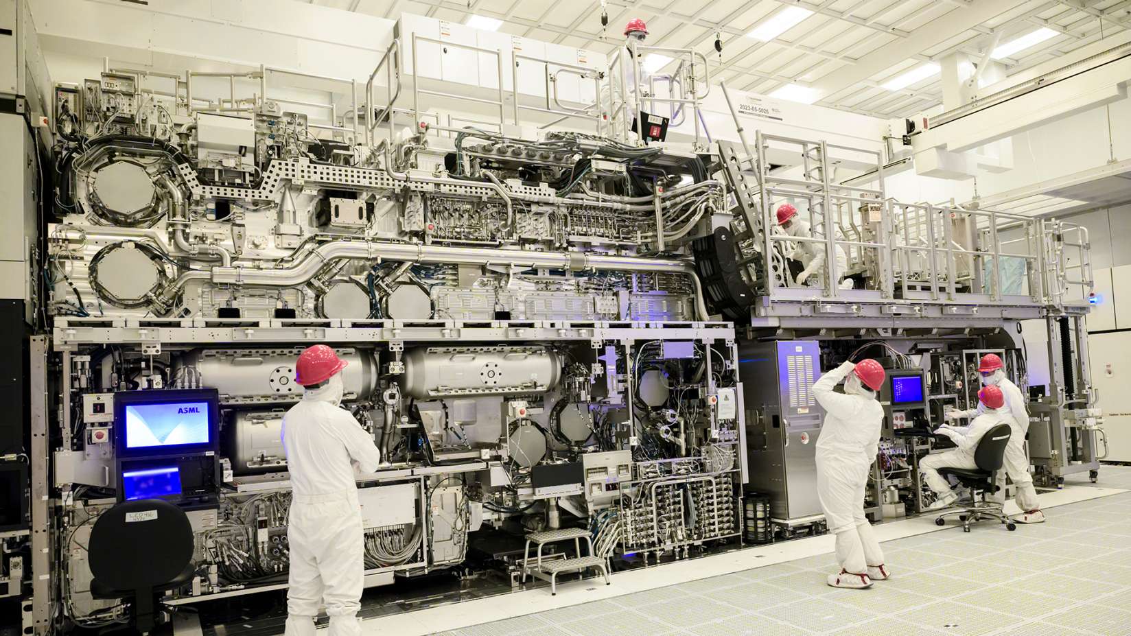
In the clean room of Intel Corporation's Fab D1X in Hillsboro, Oregon, Intel Fellow Mark Phillips briefs media on the company's High Numerical Aperture Extreme Ultraviolet lithography tool. The 165-ton High NA EUV tool was built by ASML and is the first commercial lithography system in the world. The machine will allow Intel Foundry to continue its pursuit of Moore's Law by creating for its customers powerful chips with ever-smaller transistors. (Credit: Intel Corporation)
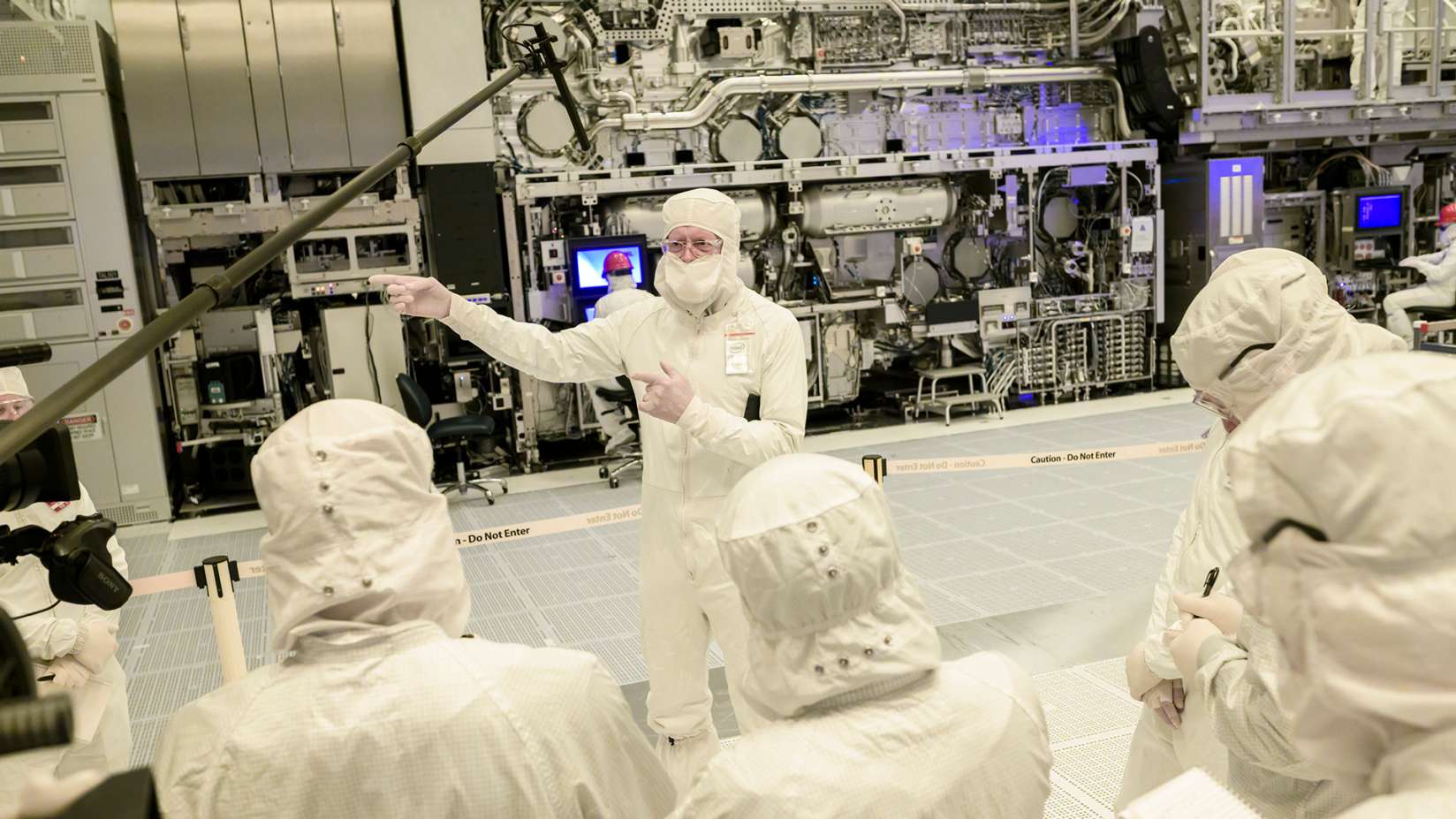
In the clean room of Intel Corporation's Fab D1X in Hillsboro, Oregon, Intel Fellow Mark Phillips briefs media on the company's High Numerical Aperture Extreme Ultraviolet lithography tool. The 165-ton High NA EUV tool was built by ASML and is the first commercial lithography system in the world. The machine will allow Intel Foundry to continue its pursuit of Moore's Law by creating for its customers powerful chips with ever-smaller transistors. (Credit: Intel Corporation)
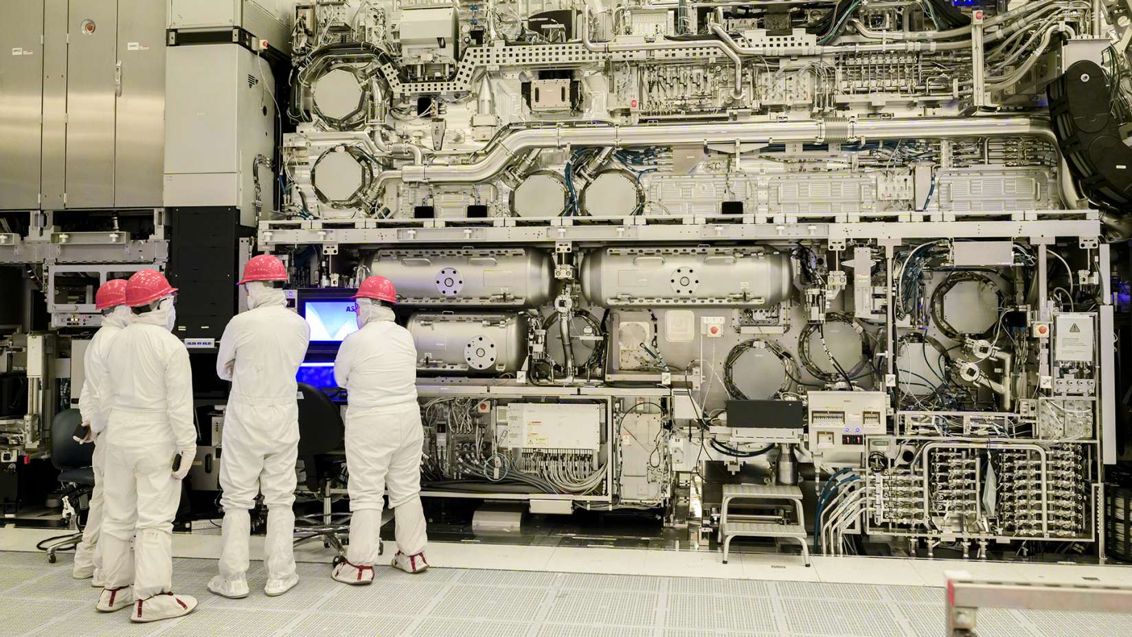
Installation is complete and calibration started on Intel's High Numerical Aperture Extreme Ultraviolet lithography tool in a clean room at Intel Corporation's Fab D1X in Hillsboro, Oregon, in April 2024. The 165-ton High NA EUV tool was built by ASML and is the first commercial lithography system of its kind in the world. The machine will allow Intel Foundry to continue its pursuit of Moore's Law by creating for its customers powerful chips with ever-smaller transistors. (Credit: Intel Corporation)
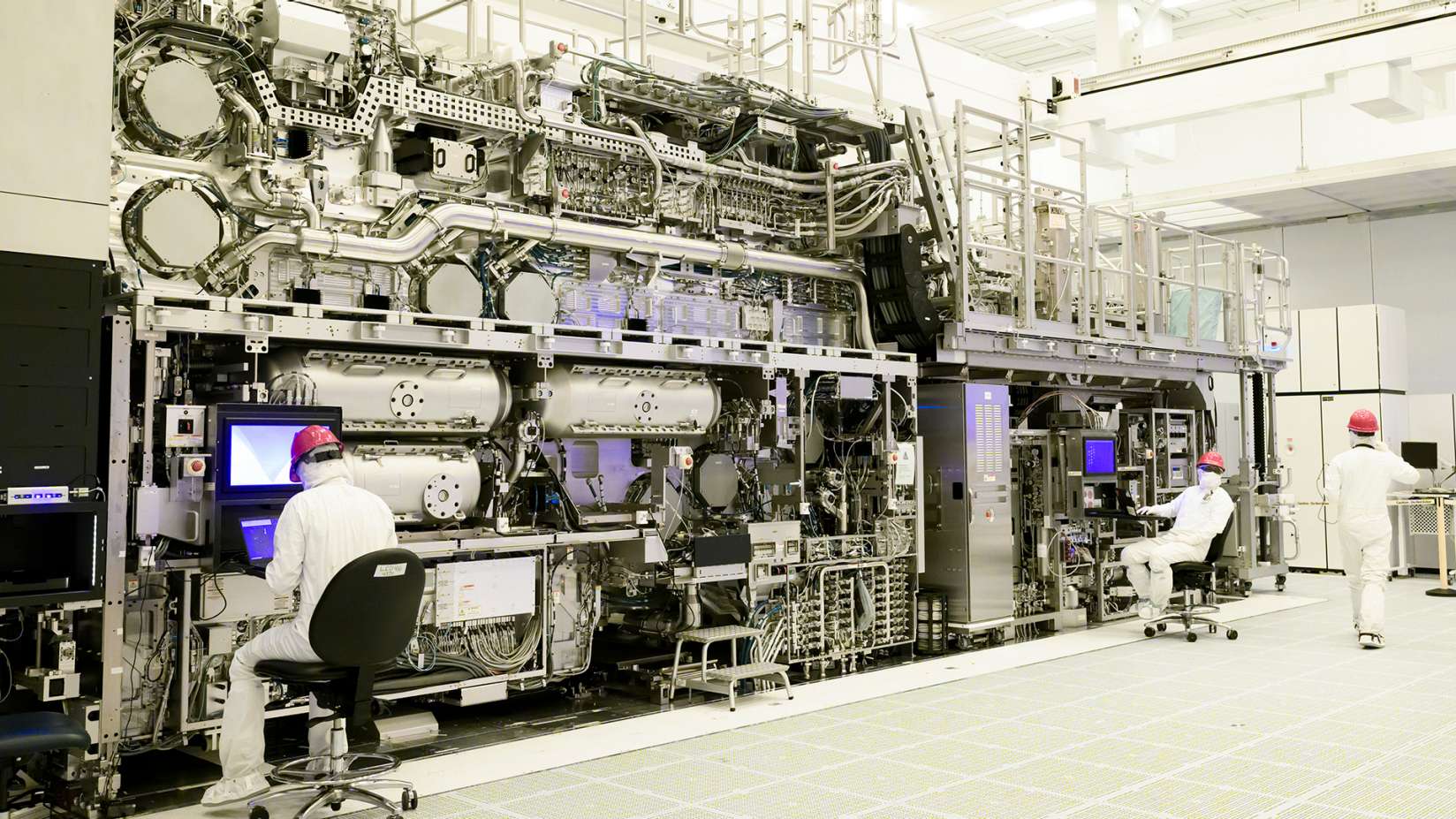
Installation is complete and calibration started on Intel's High Numerical Aperture Extreme Ultraviolet lithography tool in a clean room at Intel Corporation's Fab D1X in Hillsboro, Oregon, in April 2024. The 165-ton High NA EUV tool was built by ASML and is the first commercial lithography system of its kind in the world. The machine will allow Intel Foundry to continue its pursuit of Moore's Law by creating for its customers powerful chips with ever-smaller transistors. (Credit: Intel Corporation)
Installation is complete and calibration started on Intel's High Numerical Aperture Extreme Ultraviolet lithography tool in a clean room at Intel Corporation's Fab D1X in Hillsboro, Oregon, in April 2024. The 165-ton High NA EUV tool was built by ASML and is the first commercial lithography system of its kind in the world. The machine will allow Intel Foundry to continue its pursuit of Moore's Law by creating for its customers powerful chips with ever-smaller transistors. (Credit: Intel Corporation)
In the clean room of Intel Corporation's Fab D1X in Hillsboro, Oregon, Intel Fellow Mark Phillips briefs media on the company's High Numerical Aperture Extreme Ultraviolet lithography tool. The 165-ton High NA EUV tool was built by ASML and is the first commercial lithography system in the world. The machine will allow Intel Foundry to continue its pursuit of Moore's Law by creating for its customers powerful chips with ever-smaller transistors. (Credit: Intel Corporation)
In the clean room of Intel Corporation's Fab D1X in Hillsboro, Oregon, Intel Fellow Mark Phillips briefs media on the company's High Numerical Aperture Extreme Ultraviolet lithography tool. The 165-ton High NA EUV tool was built by ASML and is the first commercial lithography system in the world. The machine will allow Intel Foundry to continue its pursuit of Moore's Law by creating for its customers powerful chips with ever-smaller transistors. (Credit: Intel Corporation)
Installation is complete and calibration started on Intel's High Numerical Aperture Extreme Ultraviolet lithography tool in a clean room at Intel Corporation's Fab D1X in Hillsboro, Oregon, in April 2024. The 165-ton High NA EUV tool was built by ASML and is the first commercial lithography system of its kind in the world. The machine will allow Intel Foundry to continue its pursuit of Moore's Law by creating for its customers powerful chips with ever-smaller transistors. (Credit: Intel Corporation)
Installation is complete and calibration started on Intel's High Numerical Aperture Extreme Ultraviolet lithography tool in a clean room at Intel Corporation's Fab D1X in Hillsboro, Oregon, in April 2024. The 165-ton High NA EUV tool was built by ASML and is the first commercial lithography system of its kind in the world. The machine will allow Intel Foundry to continue its pursuit of Moore's Law by creating for its customers powerful chips with ever-smaller transistors. (Credit: Intel Corporation)
Download all images (ZIP, 23 MB)
Intel Adds ASML’s First High NA EUV Tool to Oregon Factory
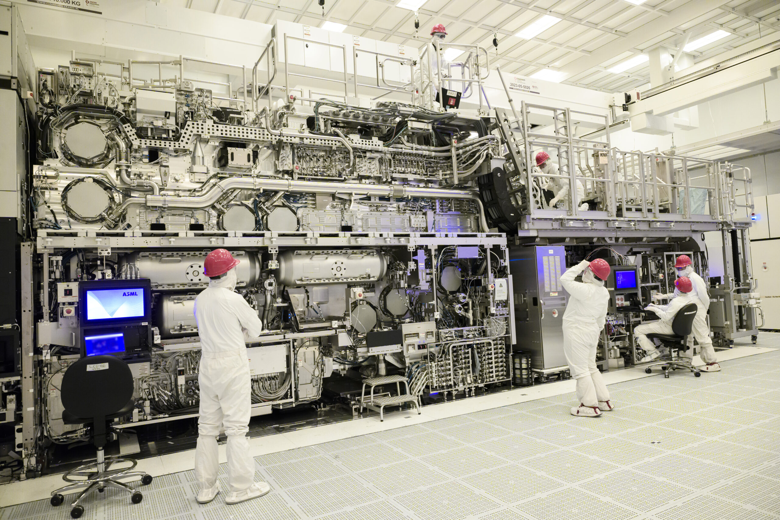
ASML’s High Numerical Aperture (High NA) Extreme Ultraviolet (EUV) lithography scanner sits in Intel Oregon’s D1X test manufacturing factory, where it is going through its final calibration. It is as big as a double-decker bus and weighs as much as a blue whale. It will shoot lasers at light speed and heat plasma to nearly 220,000 degrees Celsius, almost 40 times hotter than the surface temperature of the sun. The new TWINSCAN EXE: 5000 has the ability to dramatically improve resolution feature scaling for next-generation processors and will enable the continued pursuit of Moore’s Law. (Credit: Intel Corporation)
 www.intel.com
High NA EUV is the next-generation lithography system developed by ASML following decades of collaboration with Intel. As the first mover on High NA EUV, Intel Foundry will be able to deliver never-before-seen precision and scalability in chip manufacturing. This in turn will allow Intel to develop chips with the most innovative features and capabilities – processors that are essential for driving advancements in AI and other emerging technologies.
News
- News Byte: With High NA EUV, Intel Foundry Opens New Frontier in Chipmaking
- News: First EUV Light Marks Intel 4 Milestone in Ireland
- News: Intel and ASML Strengthen their Collaboration to Drive High-NA into Manufacturing in 2025
- Video: EUV: The Most Precise, Complex Machine at Intel
Infographic
Download full infographic
Images
In the clean room of Intel Corporation's Fab D1X in Hillsboro, Oregon, Intel Fellow Mark Phillips briefs media on the company's High Numerical Aperture Extreme Ultraviolet lithography tool. The 165-ton High NA EUV tool was built by ASML and is the first commercial lithography system in the world. The machine will allow Intel Foundry to continue its pursuit of Moore's Law by creating for its customers powerful chips with ever-smaller transistors. (Credit: Intel Corporation)
In the clean room of Intel Corporation's Fab D1X in Hillsboro, Oregon, Intel Fellow Mark Phillips briefs media on the company's High Numerical Aperture Extreme Ultraviolet lithography tool. The 165-ton High NA EUV tool was built by ASML and is the first commercial lithography system in the world. The machine will allow Intel Foundry to continue its pursuit of Moore's Law by creating for its customers powerful chips with ever-smaller transistors. (Credit: Intel Corporation)
Installation is complete and calibration started on Intel's High Numerical Aperture Extreme Ultraviolet lithography tool in a clean room at Intel Corporation's Fab D1X in Hillsboro, Oregon, in April 2024. The 165-ton High NA EUV tool was built by ASML and is the first commercial lithography system of its kind in the world. The machine will allow Intel Foundry to continue its pursuit of Moore's Law by creating for its customers powerful chips with ever-smaller transistors. (Credit: Intel Corporation)
Installation is complete and calibration started on Intel's High Numerical Aperture Extreme Ultraviolet lithography tool in a clean room at Intel Corporation's Fab D1X in Hillsboro, Oregon, in April 2024. The 165-ton High NA EUV tool was built by ASML and is the first commercial lithography system of its kind in the world. The machine will allow Intel Foundry to continue its pursuit of Moore's Law by creating for its customers powerful chips with ever-smaller transistors. (Credit: Intel Corporation)
Installation is complete and calibration started on Intel's High Numerical Aperture Extreme Ultraviolet lithography tool in a clean room at Intel Corporation's Fab D1X in Hillsboro, Oregon, in April 2024. The 165-ton High NA EUV tool was built by ASML and is the first commercial lithography system of its kind in the world. The machine will allow Intel Foundry to continue its pursuit of Moore's Law by creating for its customers powerful chips with ever-smaller transistors. (Credit: Intel Corporation)
In the clean room of Intel Corporation's Fab D1X in Hillsboro, Oregon, Intel Fellow Mark Phillips briefs media on the company's High Numerical Aperture Extreme Ultraviolet lithography tool. The 165-ton High NA EUV tool was built by ASML and is the first commercial lithography system in the world. The machine will allow Intel Foundry to continue its pursuit of Moore's Law by creating for its customers powerful chips with ever-smaller transistors. (Credit: Intel Corporation)
In the clean room of Intel Corporation's Fab D1X in Hillsboro, Oregon, Intel Fellow Mark Phillips briefs media on the company's High Numerical Aperture Extreme Ultraviolet lithography tool. The 165-ton High NA EUV tool was built by ASML and is the first commercial lithography system in the world. The machine will allow Intel Foundry to continue its pursuit of Moore's Law by creating for its customers powerful chips with ever-smaller transistors. (Credit: Intel Corporation)
Installation is complete and calibration started on Intel's High Numerical Aperture Extreme Ultraviolet lithography tool in a clean room at Intel Corporation's Fab D1X in Hillsboro, Oregon, in April 2024. The 165-ton High NA EUV tool was built by ASML and is the first commercial lithography system of its kind in the world. The machine will allow Intel Foundry to continue its pursuit of Moore's Law by creating for its customers powerful chips with ever-smaller transistors. (Credit: Intel Corporation)
Installation is complete and calibration started on Intel's High Numerical Aperture Extreme Ultraviolet lithography tool in a clean room at Intel Corporation's Fab D1X in Hillsboro, Oregon, in April 2024. The 165-ton High NA EUV tool was built by ASML and is the first commercial lithography system of its kind in the world. The machine will allow Intel Foundry to continue its pursuit of Moore's Law by creating for its customers powerful chips with ever-smaller transistors. (Credit: Intel Corporation)
Download all images (ZIP, 23 MB)
Intel Adds ASML’s First High NA EUV Tool to Oregon Factory
ASML’s High Numerical Aperture (High NA) Extreme Ultraviolet (EUV) lithography scanner sits in Intel Oregon’s D1X test manufacturing factory, where it is going through its final calibration. It is as big as a double-decker bus and weighs as much as a blue whale. It will shoot lasers at light speed and heat plasma to nearly 220,000 degrees Celsius, almost 40 times hotter than the surface temperature of the sun. The new TWINSCAN EXE: 5000 has the ability to dramatically improve resolution feature scaling for next-generation processors and will enable the continued pursuit of Moore’s Law. (Credit: Intel Corporation)
Press Kit: High NA EUV at Intel
Intel is industry’s first mover on High NA EUV lithography system.
www.intel.com