EUV process 'fades out' in next-generation memory, foundries use it from '1.4nm'
Samsung Electronics and SK Hynix are moving to postpone the introduction of ASML's 'high numerical aperture (NA) extreme ultraviolet (EUV)' equipment for the DRAM exposure process. This is due to the astronomical price of the equipment and the expected changes in the DRAM structure in the future.
Samsung Electronics and SK Hynix are planning to mass produce 3D DRAMs after 2030. They plan to use argon fluoride (ArF) equipment, not EUV equipment, for the 3D DRAM exposure process. For this reason, the introduction of high NA EUV equipment is bound to be a burden for chipmakers.
Next-generation memory '3D DRAM' not utilizing EUV process
According to the industry on the 15th, Samsung Electronics will preemptively apply high NA EUV equipment to its foundry. It is reported that they are considering whether to apply it to the 10nm 7th generation DRAM (1d DRAM) in the DRAM process or to mass production of vertical channel transistor (VCT) DRAMs. The reason
memory companies are taking a conservative stance on the introduction of high NA EUV is due to the future DRAM roadmap. According to the DRAM roadmap of Samsung Electronics and SK Hynix, the memory architecture will change in the order of 6F square DRAM → 4F square DRAM → 3D DRAM.
Among these, the 3D DRAM exposure process does not require the use of high NA EUV equipment or low NA EUV equipment. 3D DRAM is a memory concept that vertically stacks DRAM cells like NAND. While existing DRAMs have increased transistors through fine processes, 3D DRAM expands transistors through vertical stacking. Therefore, ArF equipment, not EUV equipment, is used for the exposure process.
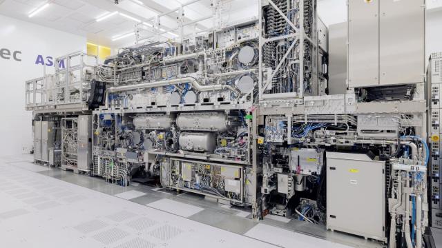
ASML's high-NA EUV equipment. Photo: ASML
This means that even if the latest equipment worth over 500 billion won is introduced, the time that it can be used for cutting-edge DRAM mass production will not be long. However, the 4F Square DRAM that both companies plan to mass-produce in the late 2020s is likely to use high-NA EUV equipment. Samsung Electronics calls it VCT DRAM and SK Hynix calls it vertical gate (VG) DRAM, which requires an EUV process for mass production of this memory.
SK Hynix is taking a similar stance to Samsung Electronics on the introduction of high-NA EUV. In particular, it has been understood that SK Hynix is reviewing the introduction of equipment more carefully than Samsung Electronics since it must use high-NA EUV equipment only for the memory process.
An official familiar with Samsung Electronics' next-generation DRAM development issues explained, "I understand that Samsung Electronics has postponed the completion date of 3D DRAM development from the original 2030 to 2032~2033," adding, "Since 3D DRAM has a completely new structure, the related ecosystem has not been established yet." He added, "The existing vertical deposition and etching need to be converted to horizontal, but this technological difficulty is considerable." "The materials have isotropic properties, so it is not easy to control."
High-NA EUV equipment, targeting application to '1.4nm' in foundries
High-NA EUV equipment will be utilized first in the foundry process. However, it is expected to take some time until high-NA EUV is applied to mass production. ASML predicted that high-NA EUV equipment will be applied to mass production processes after 2027.
Currently, the three foundries that have received high-NA EUV equipment from ASML are Intel, TSMC, and Samsung Electronics. All of this equipment is for R&D, not mass production.
It has been confirmed that Samsung Electronics is developing the process assuming that high-NA EUV equipment will be used in the foundry 1.4nm process. Samsung Electronics is aiming for mass production of the 1.4nm process in 2027. Accordingly, the high NA EUV equipment 'EXE:5000' that Samsung Electronics is currently setting up at NRD-K will also be used primarily for R&D purposes.
TSMC is delaying the use of the high NA EUV equipment as much as possible. At a recent event, it was announced that the plan is to use the high NA EUV equipment starting from the derivative process A14P, not A14 (1.4 nm). This is not unrelated to the price of the high NA EUV equipment.
 www.thebell.co.kr
Samsung Electronics and SK Hynix are moving to postpone the introduction of ASML's 'high numerical aperture (NA) extreme ultraviolet (EUV)' equipment for the DRAM exposure process. This is due to the astronomical price of the equipment and the expected changes in the DRAM structure in the future.
Samsung Electronics and SK Hynix are planning to mass produce 3D DRAMs after 2030. They plan to use argon fluoride (ArF) equipment, not EUV equipment, for the 3D DRAM exposure process. For this reason, the introduction of high NA EUV equipment is bound to be a burden for chipmakers.
Next-generation memory '3D DRAM' not utilizing EUV process
According to the industry on the 15th, Samsung Electronics will preemptively apply high NA EUV equipment to its foundry. It is reported that they are considering whether to apply it to the 10nm 7th generation DRAM (1d DRAM) in the DRAM process or to mass production of vertical channel transistor (VCT) DRAMs. The reason
memory companies are taking a conservative stance on the introduction of high NA EUV is due to the future DRAM roadmap. According to the DRAM roadmap of Samsung Electronics and SK Hynix, the memory architecture will change in the order of 6F square DRAM → 4F square DRAM → 3D DRAM.
Among these, the 3D DRAM exposure process does not require the use of high NA EUV equipment or low NA EUV equipment. 3D DRAM is a memory concept that vertically stacks DRAM cells like NAND. While existing DRAMs have increased transistors through fine processes, 3D DRAM expands transistors through vertical stacking. Therefore, ArF equipment, not EUV equipment, is used for the exposure process.
ASML's high-NA EUV equipment. Photo: ASML
This means that even if the latest equipment worth over 500 billion won is introduced, the time that it can be used for cutting-edge DRAM mass production will not be long. However, the 4F Square DRAM that both companies plan to mass-produce in the late 2020s is likely to use high-NA EUV equipment. Samsung Electronics calls it VCT DRAM and SK Hynix calls it vertical gate (VG) DRAM, which requires an EUV process for mass production of this memory.
SK Hynix is taking a similar stance to Samsung Electronics on the introduction of high-NA EUV. In particular, it has been understood that SK Hynix is reviewing the introduction of equipment more carefully than Samsung Electronics since it must use high-NA EUV equipment only for the memory process.
An official familiar with Samsung Electronics' next-generation DRAM development issues explained, "I understand that Samsung Electronics has postponed the completion date of 3D DRAM development from the original 2030 to 2032~2033," adding, "Since 3D DRAM has a completely new structure, the related ecosystem has not been established yet." He added, "The existing vertical deposition and etching need to be converted to horizontal, but this technological difficulty is considerable." "The materials have isotropic properties, so it is not easy to control."
High-NA EUV equipment, targeting application to '1.4nm' in foundries
High-NA EUV equipment will be utilized first in the foundry process. However, it is expected to take some time until high-NA EUV is applied to mass production. ASML predicted that high-NA EUV equipment will be applied to mass production processes after 2027.
Currently, the three foundries that have received high-NA EUV equipment from ASML are Intel, TSMC, and Samsung Electronics. All of this equipment is for R&D, not mass production.
It has been confirmed that Samsung Electronics is developing the process assuming that high-NA EUV equipment will be used in the foundry 1.4nm process. Samsung Electronics is aiming for mass production of the 1.4nm process in 2027. Accordingly, the high NA EUV equipment 'EXE:5000' that Samsung Electronics is currently setting up at NRD-K will also be used primarily for R&D purposes.
TSMC is delaying the use of the high NA EUV equipment as much as possible. At a recent event, it was announced that the plan is to use the high NA EUV equipment starting from the derivative process A14P, not A14 (1.4 nm). This is not unrelated to the price of the high NA EUV equipment.
삼성·SK, '하이 NA EUV' 달라진 투자 셈법
삼성전자와 SK하이닉스가 D램 노광 공정에 ASML의 '하이 개구수(NA) 극자외선(EUV)' 장비 도입을 미루려는 움직임을 보이고 있다. 천문학적인 장비 가격과 향후 예정된 D램 구조 변화 때문이다.삼성전자와 SK하이닉스 2030년 이후 3D D...
 Remember, these systems cost $380M each and you will need a dozen of them per fab for full HNA-EUV? That is a big expense for a new foundry that is trying to break even in 2027.