China uses groundbreaking desktop-sized EUV light source to make 14-nanometre chips
Hefei-based company improves manufacture of the semiconductors used to power industrial automation and electric carsZhang Tong in Beijing
Published: 2:00pm, 21 Nov 2025
Updated: 6:27pm, 21 Nov 2025
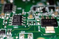
Chinese scientists and engineers are shrinking one of the most complex and expensive technologies in modern chipmaking down to desktop size and using it to manufacture 14-nanometre chips.
While 14-nm chips no longer represent the cutting edge – commercial foundries have already pushed into the 3-nm realm – they remain a sweet spot for performance, cost and efficiency, powering everything from industrial automation to electric vehicles and smart wearables.
At the UltrafastX academic conference in late October, Hefei Lumiverse Technology, based in Anhui province, central China, unveiled an extreme ultraviolet (EUV) light source technology.
“We specialise in semiconductor inspection and quantum chip manufacturing. One of our industrial clients has already utilised this light source to produce 14-nm chips,” a company spokesman said this week. (Fred's note: this is probably for metrology and/or inspection, see below)
EUV light sources are a critical component of the lithography machines used to manufacture chips with processes below 7nm, but they can be incredibly complex, massive and expensive. For example, industry leader ASML’s NXE:3400B is about 12 metres (39 feet) long and 4 metres high.
The laser-produced plasma (LPP) method used by ASML fires a laser at tin droplets to generate plasma, resulting in EUV light with a wavelength of 13.5nm. But the system costs more than US$100 million, according to the spokesman.
“This LPP method also requires specialised collector mirrors, which currently cannot be produced domestically in China,” he added.
In contrast, the Lumiverse technology is based on high-harmonic generation (HHG), a method that directs a high-precision femtosecond laser into an inert gas – typically argon – to generate high-order harmonics, producing coherent EUV light.
Internationally, ASML and other industry giants like Intel, Samsung and Taiwan Semiconductor Manufacturing Company (TSMC) have already begun to adopt HHG technology for metrology and inspection applications.
Advantages include significantly lower equipment and maintenance costs, as well as the ability to tune the wavelength of the generated light across a broad range, from 1nm to 200nm, according to the Lumiverse spokesman.
A current limitation is output power. The conversion of laser energy into light achieves an inefficient 13.5nm EUV power output of only 1 microwatt – vastly different from the more than 200 watts required for commercial lithography machines.
However, the small exposure window means the brightness per unit area is comparable to that of large-scale machines, despite a conversion efficiency of around one millionth. In contrast, commercial LPP systems can achieve up to 6 per cent efficiency.
“While not suitable for mass production, it enables small-batch production or technical verification. Its cost is merely 1 per cent of that of a large free-electron laser facility,” the spokesman added.
“Our HHG-EUV can be used for real-time, non-destructive inspection of photomask defects and overlay errors, thereby improving the yield rate of lithography processes,” he said.
“Furthermore, because the light is coherent, it can be used with coherent diffractive imaging algorithms to probe 3D structures. This allows for the examination of critical transistor architectures, such as FinFETs at the 14-nm and 7-nm nodes, and the newer gate-all-around transistors at the 3nm node.”
The spokesman said that about 80 per cent of the company’s clients were academic users. “Researchers use our desktop-sized devices to perform advanced studies, such as etching intricate quantum chips, in their own labs, bypassing the need for large-scale facilities.”
Since it was founded in late 2023, the company has assembled a core team that includes researchers from China’s Thousand Talents Plan and engineering experts with extensive international industry experience.
Its chief scientist previously served as the head of EUV laser technology at US-based KMLabs, where he led the team that developed and commercialised the world’s first HHG-based EUV femtosecond laser.
The company currently holds an internationally leading position in the specific 13.5nm EUV domain, the spokesman said.
“The next goal is to increase the output power to 1 milliwatt and expand the illumination area to enhance inspection efficiency so that we can enter the chip inspection market,” he added.
“While overseas competitors like Germany’s AFS (Active Fibre Systems) also claim 1mW EUV output, their technology operates at a longer wavelength of around 50nm, which is considered less challenging to achieve than the critical 13.5nm required for advanced chipmaking.”
https://www.scmp.com/news/china/sci...sktop-sized-euv-light-source-make-14-nm-chips
Attachments
Last edited by a moderator: