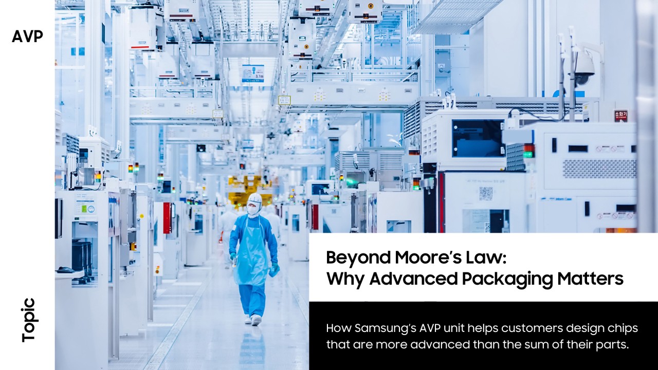
How Samsung’s Advanced Packaging business team helps customers design chips with higher density and performance than the sum of their parts.
The fundamental principle of semiconductor scaling over the last five decades has been Moore’s Law. First put forward by Gordon Moore in 1965, this maxim predicts that the density of the transistors you can fit on a chip doubles roughly every 24 months, leading to greater speed and power efficiency.But times are changing. Moore’s Law is slowing down, and chip miniaturization is approaching its limits. The market is also increasingly demanding more versatile semiconductors, such as ones that package additional features like RF wireless communications, high bandwidth memory, and logic into a single chip.
For these reasons, it is becoming difficult to continue to scale semiconductor performance and efficiency through process miniaturization alone. With today’s era of high-performance applications like AI and hyperscale computing putting more pressure on the industry than ever, we need to be innovative to keep up.
Enter advanced packaging, and Samsung's Advanced Packaging (AVP) business team.
What is Advanced Packaging?
In semiconductors, packaging refers to the process in which one or more components or integrated circuits are placed in a casing made of a material like metal, plastic, glass, ceramic, and so on. In plain language, the entirety of the package is what we think of as the ‘computer chip.’
When chips first started being manufactured in the 1950s, integrated circuits on silicon wafers were packaged by connecting them to the printed circuit board (PCB) with solder and thin metal wires. However, starting in the 90s, packaging began to evolve, with this wire-bond interconnection technique phased out in favor of flip-chip. In flip-chip, the entire surface area of the silicon wafer is used for interconnection with the PCB through solder bumps and an integrated-circuit substrate. This was then followed by wafer level packaging, in which chips were packaged as part of the silicon wafer itself using a redistribution layer (RDL) and then diced apart by a laser, with no substrate between the die and the PCB.
Advanced packaging takes this evolution to the next level. In a 2.5D package, a single-layer logic semiconductor and multi-layer memory semiconductors are indirectly attached to the package substrate through an interposer layer like RDL, silicon bridge, through-silicon via (TSV) or glass. This creates greater flexibility in combining different functionalities on a single package. After that, there’s 3D packaging, in which multiple logic and memory semiconductors are vertically integrated. This results in shorter interconnects, smaller package footprints, and enhanced performance and functionality.
X-Cube, I-Cube, and Heterogeneous Integration
The key to making advanced packaging work is called heterogeneous Integration.
Heterogeneous Integration Technology brings chips, process nodes, and bleeding-edge technologies together in one unified package— increasing density and combining powerful functions. Through this process, separately manufactured components (for example, a logic semiconductor and memory semiconductors) are integrated into a higher-level assembly called system-in-package (SIP). Through advanced heterogeneous integration, multiple chips can be connected both horizontally and vertically, allowing more transistors to be packed into a single package and offering performance that is greater than the sum of its parts.
Samsung AVP’s major heterogeneous integration technologies are called I-Cube and X-Cube and are based on a 2.5D and 3D package, respectively.
I-Cube deploys parallel horizontal chip placement to boost performance while combating heat build-up. TSV, and Backend-of-the-line (BEOL) technologies form a foundation for two or more chips to harmonize their specialized functions, delivering powerful solutions for modern devices. With X-Cube, stacking components vertically uses much shorter interconnect wire lengths, packing more transistors in and increasing efficiency, while saving massive amounts of on-chip real estate. This enables high system performance with lower cost while retaining high bandwidth and low power.
Conclusion
In a future powered by high bandwidth memory and advanced computing, advanced package technology like I-Cube and X-Cube is empowering device manufacturers to explore innovative technologies that push the limits of performance in their products. By working with Samsung’s AVP business team, they can create custom chips by combining multiple components from Samsung’s IP profile, then combining them into a single package.
The result? Advanced custom chips custom-tailored for innovative new industries like HPC, AI, Automotive, and more. Moore’s Law might well be slowing down. But thanks to AVP, Samsung Semiconductor’s chips aren’t slowing down with it.
Beyond Moore’s Law: Why Advanced Packaging Matters
Beyond Moore’s Law: Why Advanced Packaging Matters How Samsung’s Advanced Packaging business team helps customers design chips with higher density and performance than the sum of their parts. The fundamental principle of semiconductor scaling over the last five decades has been Moore’s Law.
 www.linkedin.com