Array
(
    [content] => 
    [params] => Array
        (
            [0] => /forum/threads/can-intel-recover-even-part-of-their-past-dominance.23972/page-3
        )

    [addOns] => Array
        (
            [DL6/MLTP] => 13
            [Hampel/TimeZoneDebug] => 1000070
            [SV/ChangePostDate] => 2010200
            [SemiWiki/Newsletter] => 1000010
            [SemiWiki/WPMenu] => 1000010
            [SemiWiki/XPressExtend] => 1000010
            [ThemeHouse/XLink] => 1000970
            [ThemeHouse/XPress] => 1010570
            [XF] => 2030770
            [XFI] => 1060170
        )

    [wordpress] => /var/www/html
)

Can Intel recover even part of their past dominance?

Beyond a given point, lowering voltage further increases power consumption per operation.

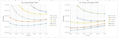
If you look at power-delay product, this tells you the energy needed to do something, Dynamic power (CV^2) drops with lower voltages (leakage less so) but so does clock speed, more rapidly as you get closer to the threshold voltages. For a given gate type (e.g. ELVT, ULVT, LVT, SVT) and clock speed (and activity percentage) there is a supply voltage where PDP reaches a minimum, and this where the power consumption is also a minimum -- as VDD drops you have to run slower but with more parallel circuits, which works for many things but not all. And if you're really bothered about power efficiency, you also need to vary VDD with process corner and temperature, and also circuit activity and clock speed.

For the circuits we've looked at in N3 and N2 which are relatively high activity (e.g. DSP, FEC...) the lowest PDP is usually with ELVT, but has never been as low as 0.225V -- for lower activity circuits where ELVT leakage is too high compared to dynamic power, ULVT can be better. But there's no single "best" answer (transistor type, voltage, frequency), it all depends on what the circuits are doing... ;-)
Electricity accounts 80% of BTC mining cost.
You can try a better solution and there's a lot of money to be made .
Intel was once a wantobe player.
 
Electricity accounts 80% of BTC mining cost.
You can try a better solution and there's a lot of money to be made .
Intel was once a wantobe player.
Which is true -- I was trying to correct the misapprehension that lower voltage is always better for efficiency/energy use, because it's not. However the minimum PDP VDD is well below anything used by chips like CPUs and GPUs today where lower voltage does always improve efficiency, depending on process corner (and circuit, and clock speed, and activity, and transistor type, and phase of the moon...) it's usually around 0.4V or a bit lower which is in the depths far below where CPUs lurk... ;-)

But you can't just take a chip designed for "normal-voltage" operation and drop the supply voltage massively because it won't work, at least not reliably -- if you want to operate down in this region you need to use special libraries and also tool precautions and new timing checks, because gate delay variation and sensitivity to supply voltage drops gets rapidly worse. TSMC enforce special rules for ULV operation, and the voltage where this happens varies with transistor type (ELVT, ULVT, LVT, SVT) -- which then causes bigger issues with mixing transistor types (e.g. uncorrelated Vth) because the delay tracking between types gets worse and worse.

All this imposes some penalties on design which reduce performance and increase area (as does going slower and more parallel), so you don't want to do this for a chip which spends most of its time (and dissipates most of its power) at higher Vdd (e.g. 0.5V and above) like a CPU. However if you have a chip which has one job to do and where power consumption is all-important and you're willing to use adaptive supply voltage, it's a price worth paying -- we've been doing this for some time now, the typical power saving is similar to a complete process node step, and the worst-case saving is closer to two process nodes... :-)
 
If Intel design an SRAM that scales, they could regain the lead. But SRAM is like other memory, scaling seems to have ended. SRAM is 90% of the area of a logic chip.

This leads to an observation, who knows memory better than Samsung? Maybe Samsung is a dark horse in the battle to scale SRAM.
 
Here is the story:

HP had a big R&D group which spun out Agilent Technologies which became Avago. This was Hock Tan's doing. Avago had an IP group that had the lead in SerDes and other IP so based on that IP Avago did custom ASICs. This was back when IBM, LSI Logic, VLSI Technologies, NEC, and other Japanese semiconductor companies owned the ASIC market. IBM really was a force of nature back then. Avago bought LSI Logic, GlobalFoundries bought IBM Semiconductor and there was other consolidation. Avago became Broadcom, again Hock Tan's doing, and the ASIC business grew. Last I heard it was $30B+ of BRCM revenue.

Avago did Google's first TPUs but Google built up internal teams so they do most of their own design now. Avago still handles some of the backend stuff. I worked for an EDA company who was inside Google for 16nm, 7nm, 5nm, and 3nm. The TSMC N2 TPU is now in process.. They wrote some very big checks and are a coveted EDA/IP customer. Broadcom, on the other hand, has always been cheap on EDA tools. I worked on a couple of projects with them back in the 1990s and it was rough. From what I hear Hock Tan has continued that tradition of sharp penciling.
The analyst Beth Kindig just published a piece saying that Broadcom sells these TPUs to Google for $13,000 a piece. (not bad for just doing some of the backend stuff) There is also an order backlog of $73B in the next few quarters. (not just Google)
 
Which is true -- I was trying to correct the misapprehension that lower voltage is always better for efficiency/energy use, because it's not. However the minimum PDP VDD is well below anything used by chips like CPUs and GPUs today where lower voltage does always improve efficiency, depending on process corner (and circuit, and clock speed, and activity, and transistor type, and phase of the moon...) it's usually around 0.4V or a bit lower which is in the depths far below where CPUs lurk... ;-)

But you can't just take a chip designed for "normal-voltage" operation and drop the supply voltage massively because it won't work, at least not reliably -- if you want to operate down in this region you need to use special libraries and also tool precautions and new timing checks, because gate delay variation and sensitivity to supply voltage drops gets rapidly worse. TSMC enforce special rules for ULV operation, and the voltage where this happens varies with transistor type (ELVT, ULVT, LVT, SVT) -- which then causes bigger issues with mixing transistor types (e.g. uncorrelated Vth) because the delay tracking between types gets worse and worse.

All this imposes some penalties on design which reduce performance and increase area (as does going slower and more parallel), so you don't want to do this for a chip which spends most of its time (and dissipates most of its power) at higher Vdd (e.g. 0.5V and above) like a CPU. However if you have a chip which has one job to do and where power consumption is all-important and you're willing to use adaptive supply voltage, it's a price worth paying -- we've been doing this for some time now, the typical power saving is similar to a complete process node step, and the worst-case saving is closer to two process nodes... :-)
you certainly cannot just scale Vdd and expect the original HPC application to scale. the call for 0.25v Vdd is about getting to the power efficiency for the same workload, hence requires device and architecture innovations
 
you certainly cannot just scale Vdd and expect the original HPC application to scale. the call for 0.25v Vdd is about getting to the power efficiency for the same workload, hence requires device and architecture innovations
And as I said there's an optimum voltage for lowest PDP (power-delay product), and in my experience (all transistor types, N7 down to N2) it's never as low as 0.25V even with ELVT transistors -- that's from extensive evaluation using real cell libraries across a wide range of conditions.

Yes you can get very low power consumption per gate because dynamic power (CV^2) always drops as you reduce voltage, but once you get below the optimum-PDP voltage -- which is invariably bigger than the sum of the NMOS and PMOS Vths -- delay goes up faster than power drops, so power for the same workload increases. Lower-Vth transistors like ELVT have a lot more leakage, so especially in lower-activity/lower-clock-rate circuits these can make things worse, not better.

No magic device/architecture wand possible here, it's a fundamental property of CMOS transistors -- and the voltages have only moved down slightly over several process nodes, because the shape of the Ids vs. Vgs curves has hardly changed, and neither has subthreshold slope -- Nanosheets in N2 instead of FinFETs show a small improvement, but not that significant.

Here's an old example for N7, so not giving anything secret away... ;-)
 

Attachments

  • PDP.jpg
    PDP.jpg
    69.7 KB · Views: 29
Last edited:
The analyst Beth Kindig just published a piece saying that Broadcom sells these TPUs to Google for $13,000 a piece. (not bad for just doing some of the backend stuff) There is also an order backlog of $73B in the next few quarters. (not just Google)

Compare that to what Nvidia charges......... $13k seems to be pretty cheap.

How many TPU chips does Broadcom do for Google per year? Hundreds of thousands versus millions?

Google has (2) N2 designs in progress that I am aware of. Once the design is complete Google then hands over functionally verified RTL to Broadcom or MediaTek for implementation, packaging and testing. The chips use CoWos so TSMC is also a collaborator in this.

Some ASIC companies do the complete design from spec to chip. Some get GDSII and have the chips made, Google is a hybrid where they do the design, integrate IP, run simulations based on the PDKs, and do functional verification. It really is a close collaboration between the customer, ASIC partner, and foundry.
Broadcom CEO said the order backlog for the next 6 quarters is $73B for AI processors. (those are confirmed orders -- there will be additional orders -- total will be higher)

$13,000 / device just to do "some backend stuff" ... doesn't sound cheap. Also, Broadcom gross margins (all products) are 78%.
I have heard from multiple sources Google's own design teams are taking over more and more of TPU design. Anyone has more specifics on which TPU version this started and the % of partition labor?
 
And as I said there's an optimum voltage for lowest PDP (power-delay product), and in my experience (all transistor types, N7 down to N2) it's never as low as 0.25V even with ELVT transistors -- that's from extensive evaluation using real cell libraries across a wide range of conditions.

Yes you can get very low power consumption per gate because dynamic power (CV^2) always drops as you reduce voltage, but once you get below the optimum-PDP voltage -- which is invariably bigger than the sum of the NMOS and PMOS Vths -- delay goes up faster than power drops, so power for the same workload increases. Lower-Vth transistors like ELVT have a lot more leakage, so especially in lower-activity/lower-clock-rate circuits these can make things worse, not better.

No magic device/architecture wand possible here, it's a fundamental property of CMOS transistors -- and the voltages have only moved down slightly over several process nodes, because the shape of the Ids vs. Vgs curves has hardly changed, and neither has subthreshold slope -- Nanosheets in N2 instead of FinFTEs show a small improvement, but not that significant.

Here's an old example for N7, so not giving anything secret away... ;-)
You're correct for most chips, but not for BTC ASICs.
The Bitmain 7 nm miner is called the S19 or S19 Pro, and its chips run at around 0.32 V.
BTC chips are currently the industry leaders in achieving the lowest operating voltage and power consumption.
 
You're correct for most chips, but not for BTC ASICs.
The Bitmain 7 nm miner is called the S19 or S19 Pro, and its chips run at around 0.32 V.
BTC chips are currently the industry leaders in achieving the lowest operating voltage and power consumption.
The laws of physics apply to BTC ASICs just like they do for all others, and no amount of being "an industry leader" can get round them... ;-)

If you're willing to do things like accepting reduced yield by skewing/tightening the process window towards the FF corner then you can push the minimum-PDP voltage down, as can be seen from the RH plot I showed (which was for N7) -- but you have to take extreme care doing this because leakage goes up significantly and this increases rapidly with temperature, so you risk thermal runaway at high chip power levels on fast chips.

That's nothing to do with some super-cleverness in design or "secret sauce", it's simply a commercial decision like CPU binning. If Bitmain claim otherwise and you believe them, you're drinking their Kool-Aid... ;-)

P.S. "VDD down to 0.32V" (in the hot FF corner) is more believable, this would also be the minimum power corner -- but typical would probably be around 0.37V (and higher power) and the cold SS corner would need something like 0.43V (maybe even higher) and dissipate even more power (higher CV^2) -- because that's how CMOS works over PVT variation with adaptive supply voltages... ;-)

P.P.S. Have you ever actually been involved in real physical design in N7/N5/N4/N3/N2, to give some credibility to your statements?
 
Last edited:
Back
Top