This year's SPIE Advanced Lithography conference was held virtually due to the COVID impact on travel. While papers are now immediately available, you can get stuck waiting, from the web traffic. Also, many papers were video only.
There were a number of papers of course on probably the hottest topic, EUV. By piecing together information from some key papers, you can get some important information.
It is already worth noting that several papers focused on single exposure at the 28 nm pitch. This is no coincidence, as Samsung's 4nm foundry node and TSMC's 5 nm node have been reported to sport such a minimum metal pitch (see here: https://semiwiki.com/forum/index.ph...-for-the-foreseeable-future.13730/#post-45732).
The first piece of information is the throughput, presented in paper 11609-3: High-NA EUV Llthography exposure tool: key advantages and program progress by J. van Schoot et al.

With the field power level at 250 W, this graph can be converted to throughput vs dose:

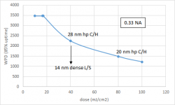
Another presentation by ASML, paper 11609-6, 0.33 NA EUV systems for high-volume manufacturing, by E. Verhoeven et al., showed the availability averaging to ~85%, so we may get wafers per day by 0.85*WPH*24, which is shown below for the 0.33 NA case only.

On the graph, the doses and corresponding WPD are noted for the 14 nm lines and spaces (L/S) case and the 20 nm hp contact hole (C/H) cases. The contact hole cases are addressed in the high-NA paper 11609-3. The 28 nm half-pitch (hp) C/H dose can be halved to produce the same width as the 20 nm hp C/H (single exposure dose is 80 mJ/cm2, for addressing stochastic defects), and two such exposures can be interleaved in double patterning to go from 28 nm hp to 20 nm hp.

The 14 nm hp L/S case is discussed in more detail in paper 11609-29, Extending 0.33 NA EUVL to 28 nm pitch using alternative mask and controlled aberrations, by D. Rio et al., which indicated that the best illumination for 28 nm pitch with conventional EUV masks only used 50% of the source power, so 250 W is effectively halved to 125 W. An attenuated phase shift mask would need to be developed to use the full 250 W. Incidentally, negative resist exposure of the areas outside the metal line locations is recommended by several papers at the conference, including 11609-29.
The best reported cases of throughput are >2000 wafers per day (in paper 11609-6). It becomes clear that 20 nm hp contact holes as well as 28 nm pitch lines and spaces are too slow as single exposures to support this reported throughput. So double patterning must be used to get the higher throughput at the larger (1.4x for C/H, 2x for L/S) pitch, with either the full source power (for L/S) or the lower dose (for C/H).
There were a number of papers of course on probably the hottest topic, EUV. By piecing together information from some key papers, you can get some important information.
It is already worth noting that several papers focused on single exposure at the 28 nm pitch. This is no coincidence, as Samsung's 4nm foundry node and TSMC's 5 nm node have been reported to sport such a minimum metal pitch (see here: https://semiwiki.com/forum/index.ph...-for-the-foreseeable-future.13730/#post-45732).
The first piece of information is the throughput, presented in paper 11609-3: High-NA EUV Llthography exposure tool: key advantages and program progress by J. van Schoot et al.
With the field power level at 250 W, this graph can be converted to throughput vs dose:
Another presentation by ASML, paper 11609-6, 0.33 NA EUV systems for high-volume manufacturing, by E. Verhoeven et al., showed the availability averaging to ~85%, so we may get wafers per day by 0.85*WPH*24, which is shown below for the 0.33 NA case only.
On the graph, the doses and corresponding WPD are noted for the 14 nm lines and spaces (L/S) case and the 20 nm hp contact hole (C/H) cases. The contact hole cases are addressed in the high-NA paper 11609-3. The 28 nm half-pitch (hp) C/H dose can be halved to produce the same width as the 20 nm hp C/H (single exposure dose is 80 mJ/cm2, for addressing stochastic defects), and two such exposures can be interleaved in double patterning to go from 28 nm hp to 20 nm hp.
The 14 nm hp L/S case is discussed in more detail in paper 11609-29, Extending 0.33 NA EUVL to 28 nm pitch using alternative mask and controlled aberrations, by D. Rio et al., which indicated that the best illumination for 28 nm pitch with conventional EUV masks only used 50% of the source power, so 250 W is effectively halved to 125 W. An attenuated phase shift mask would need to be developed to use the full 250 W. Incidentally, negative resist exposure of the areas outside the metal line locations is recommended by several papers at the conference, including 11609-29.
The best reported cases of throughput are >2000 wafers per day (in paper 11609-6). It becomes clear that 20 nm hp contact holes as well as 28 nm pitch lines and spaces are too slow as single exposures to support this reported throughput. So double patterning must be used to get the higher throughput at the larger (1.4x for C/H, 2x for L/S) pitch, with either the full source power (for L/S) or the lower dose (for C/H).
Attachments
Last edited:


