Array
(
    [content] => 
    [params] => Array
        (
            [0] => /forum/index.php?threads/intel-16nm-vs-10nm.17509/
        )

    [addOns] => Array
        (
            [DL6/MLTP] => 13
            [Hampel/TimeZoneDebug] => 1000070
            [SV/ChangePostDate] => 2010200
            [SemiWiki/Newsletter] => 1000010
            [SemiWiki/WPMenu] => 1000010
            [SemiWiki/XPressExtend] => 1000010
            [ThemeHouse/XLink] => 1000970
            [ThemeHouse/XPress] => 1010570
            [XF] => 2021370
            [XFI] => 1050270
        )

    [wordpress] => /var/www/html
)

Intel 16nm vs 10nm?

cliff

Active member
Can somebody explain the major differences between 16nm vs 10nm (besides 6nm)?
I am told they are both double patterned. True or false?
Is there more interconnect available (tighter pitches at M3 and above, more upper routing layers, etc)
Higher GM?
Lower leakage?
More SRAM density?
New exotic memory?
Lower interconnect capacitance or resistance?

From this article
https://semiengineering.com/new-patterning-options-emerging/
It seems that the major piece is the poly connecting to the gate above the diffusion, allowing pmos and nmos to get closer. This theoretically makes the standard cells tighter, but will that result in tighter P&R? Won't the user need to lower the utilization % to connect up the standard cells? How much tighter is the P&R block?

I assume the big savings is in SRAM?
Is there an exotic RAM involved that gets the huge size benefit?
Is Altera's FPGA fabric much tighter?

Is there a cost per fet benefit?

Was the change worth it?
 
Last edited:
Assuming you mean intel 16 vs intel 10nm family (rather than Samsung 10LPP family or the now out of production 10FF):
- intel 16 has no double patterning in the BEOL or MEOL, and it seems like it has bidirectional DRs but the whitepapers floating around aren't clear on this. Meanwhile intel 10nm/intel 7 has single for the upper metal layers, double patterning for some layers, and quad patterning for others.
- Both nodes have many publicized metal stack options optimized for different kinds of products.
- intel 16 by default has LL libraries because it was designed for those sorts of purposes and foundry use. 10nm family, like prior main intel nodes, is designed for high performance and efficient performance logic devices and only to be used for intel's SOCs. For this reason intel came out with what they called the "SOC" versions of these nodes with all of those nice add-ins that analog and the trailing edge intel chip designers like to have.
- I think I remember recently seeing that "SOC" versions of intel nodes added things like single fin SRAM cells, other than that I don't think they would have done any pitch shrinks for these nodes.
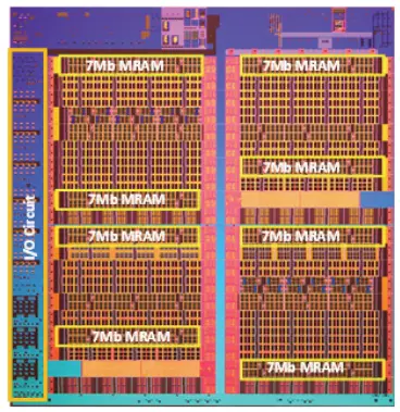
- As far as I have seen the only time intel has talked about exotic memory was MRAM and ReRAM on 22FFL (which got rebranded to intel 16 to better match it's density and performance).
- Better RC goes in the camp of interanode improvements (think the + nodes, 10nm SF, and intel 7).

Per intel's numbers intel 16 has PPW similar to 14nm++ (with the leakage being a bit higher at higher frequencies) and the densest std cell has a CH of 540nm with CPP of 108nm. Per the 22FFL whitepaper the LL library has leakage 30x lower then the best 22nm SOC LL libraries (0.5pA/µm vs 15pA/µm).

The 10nm in icelake performed similarly to 14nm++ at iso power. 10nm SF brought 18% PPW, with intel 7 bringing 10-15%, and the intel 7 in RPL seeming to bring around an additional 5%. The densest cell available has a CH of 272nm and a CPP of 54nm (note that the 54nm CPP is only found in mobile products, with the 60nm CPP being used more commonly for HP parts of mobile SOCs and the entirety of intel's desktop parts).

Another main difference is foundry interoperability. I think intel said something about how in the transformation of 22FFL to intel 16 they remastered the node for industry standard EDA tools but I could be misremembering this. For the intel 4 paper I remember intel talking about how they changed their pitch gearing and places where contacts could land to make designing for the node much easier than intel 7. I don't know how true this is but on wikichip they mentioned that the weird gearing on 10nm actually led to "skewed" std cells. To fix this problem apparently intel made a mirrored version of the cells that gets mixed in with the non mirrored version to maximize area utilization. Combine this with the draconian design rules that are probably required for the 10nm family, and I don't think it is the most designer friendly node.
 
Last edited:
Mr. NG, thank you for these answers. This was extremely helpful. Let me regurgitate...

For us potential IFS customers, we would use the rebranded 22nm, which is now called 16nm, correct? Can I call it IFS16, or is there an official name I can use?

IFS16:
- MRAM and ReRAM. Good!
- The connection between poly and M1 is in the channel/field, not over the diffusion, just like competitors?
- Single patterned M1 and above. Not as good as competitors, but can route tighter wrong-way.
- Sane (more grid like) rules, possible similar to competitors?

Does this cover it? Any other public stuff, like stacked via policies or many forbidden zones?
 
Mr. NG, thank you for these answers. This was extremely helpful. Let me regurgitate...

For us potential IFS customers, we would use the rebranded 22nm, which is now called 16nm, correct? Can I call it IFS16, or is there an official name I can use?
22FFL (the official name now being intel 16. But I just call it i16 for short) is not 22nm. Although you are certainly forgiven for the confusion the old name was terrible and the rebrands don't help matters. It is a slightly relaxed version of the 14nm fins on a slightly modified 22nm BEOL. Also according to David Kanter, intel 16 apparently has a dopant-less channel. He goes onto mention that this wasn't a thing on intel nodes until 10nm.

IFS16:
- MRAM and ReRAM. Good!
- The connection between poly and M1 is in the channel/field, not over the diffusion, just like competitors?
Are you asking if there is COAG? If so, then no. Only 10nm and beyond are COAG.
- Single patterned M1 and above. Not as good as competitors, but can route tighter wrong-way.
Even M0 and V0 are single patterned. It definitely hurts density over what you could get on say 11LPP, but per intel, the intent is for intel 16 to have similar cost and design rule complexity to 28nm, at 14nm ++ PPW, best in class leakage, and TSMC 20nm densities.
- Sane (more grid like) rules, possible similar to competitors?
Seems like it, but the papers made no specific mention of it. Although this wouldn't be surprising, because DRs probably didn't start getting crazy until 14 and 10nm.
Does this cover it? Any other public stuff, like stacked via policies or many forbidden zones?
They have also mentioned that one of the upper metal layers on intel 16 can make some killer inductors, but that stuff is way above my head. As for those DR specific things, I have never seen that sort of stuff floating around the web, nor would I be able to decipher much about it if I did see it.
 
Last edited:
Thank you again. So let's see if I can regurgitate this a little better...

IFS16 is similar to industry 28nm, but uses finfets
- higher gain. 3x perhaps?
- way lower leakage (good for dynamic logic, less refreshing, etc)
- higher poly to M1 capacitance.
- comes with an MRAM and ReRAM option (does Intel do this, or a 3rd party?)

Is M0 routed
1) horizontally in the field (channel) to connect 2 neighboring polies
2) vertically over the diffusion to connect to a backsided supply, to get to a horizonal Met1 over the diffusion, or to extend into the channel to meet with a horizontal M0 or M1?
Most 28nm processes don't have these routable diffusion/poly connection layers.

Maybe somebody can provide a ring oscillator frequency and current number.

Inductors... handling them on the interposer in the future may be a better idea

If I understand this properly, IFS16 will be popular if Intel wants to take it seriously, no?
 
Thank you again. So let's see if I can regurgitate this a little better...

IFS16 is similar to industry 28nm, but uses finfets
In wafer cost. The fact it is double patterned for the FEOL proabbly makes cost somewhere between TSMC 28nm and 16FF. Density is probably closer to 16FF than 28nm though since it is significantly denser than intel 22nm
- higher gain. 3x perhaps?
- way lower leakage (good for dynamic logic, less refreshing, etc)
- higher poly to M1 capacitance.
- comes with an MRAM and ReRAM option (does Intel do this, or a 3rd party?)
Intel fabs those options
Is M0 routed
1) horizontally in the field (channel) to connect 2 neighboring polies
2) vertically over the diffusion to connect to a backsided supply, to get to a horizonal Met1 over the diffusion, or to extend into the channel to meet with a horizontal M0 or M1?
Most 28nm processes don't have these routable diffusion/poly connection layers.
In intel terminology M0 is in the same direction as the fins and connects to the s/d and M1 is in the direction of the poly and I think it connects to the gates but I don't know. Looking at a techinsights teardown would give you a better idea about how design stuff works for intel nodes. If my assumption that with intel 16 all metal layers are bidirectional is correct, then I don't know how relevant that bit on metal line direction is though.

If I understand this properly, IFS16 will be popular if Intel wants to take it seriously, no?
I think so. If the demand is there, changing capacity over to it should be a snap too given how much is borrowed from other intel nodes.
 
Last edited:
From my understanding, there is no M0 on i16, because the M1 is still bidirectional.
90nm is around the limit for bidirectional metals with ArFi single patterning.
 
From my understanding, there is no M0 on i16, because the M1 is still bidirectional.
90nm is around the limit for bidirectional metals with ArFi single patterning.
So, they would have to have been multipattern for that metal.
 
1) Alrighty... let me word it this way. Is there a mechanism to connect parallel polies (bidirectional poly if not routable contacts, aka, M0, M1_PO, CB) without resorting to horizonal M1 in the channel

2) Is there a mechanism to extend the diffusion connection vertically into the field without resorting to M1

3) Is IFS planning on offering only 22FLL aka i16?

4) David Kantor's article in 2018 indicated that M7 and M8 are ultra wide/thick layers. IFS competitors (including GF) and below allows M7-M8 as thin as M4-8, plus 2x layers, then of course wide/thick layers above that. Has Intel expanded the number of routable (narrow) layers? Will they?
 
I don't know the answers for (1) and (2).

3) Intel will be offering Intel 16 [22FFL(++)], Intel 3 and Intel 18A. Intel 3 is an improvement over Intel 4 which was detailed at VLSI Symposium last year.

4) The previous 22FFL roadmap shows that they were looking to add a denser FEOL, denser SRAM and a denser interconnect. It's likely that added more routable layers with one of the plusses, but it's not certain until more details are out.
unknown.png
 
Thank you Redfire. Your previous comment of M1 being bidirectional has been the case for every public process (non Intel) that I know of dating back to the early 90s. That does not remove the need to have another horizontal connection layer to connect poly, because if you need to connect adjacent polies (M-factor, etc), you are forced to connect horizonally. So then how do you get across the channel (P to N)? You need to add a dummy lane, or go wrongway on M2, or waste M3 across the channel. This is standard cell layout 101.

"The previous 22FFL roadmap shows that they were looking to add a denser FEOL, denser SRAM and a denser interconnect. It's likely that added more routable layers with one of the plusses". This tells me that Intel will probably add horizonal and vertical routing capability below M1 so we can route M1 vertically across the channel without too much disruption. They will also add diffusion and poly cuts, etc. Is this correct?
Memory compilers (on slide). Just SRAM, or MRAM, ReRAM, other?

"... but it's not certain until more details are out." So that is why I am not finding the information publicly for a TSMC16 / GF14 competitive public process that has been available (by TSMC and GF) to use since 2016?
Nish provided very minor assistance by pointing me to a site (Mosis) that wanted $10K to see the most fundamental information, like how many layers, which should be shown on Intel's IFS site. Side note: Screw you Mosis. You drove companies to go to Europractice. I understand that you are relying on the corrupt university system, but that is another thread for another day.

Shouldn't the IFS marketing group respond to this chat? What is their purpose? Perhaps lobbying congress. Maybe they are good at that.
 
That roadmap is so old that wouldn’t this stuff be done or scrapped by now?
I would expect so, but we don't know the details of how it was implemented if it was, and what was scrapped if it was.

Thank you Redfire. Your previous comment of M1 being bidirectional has been the case for every public process (non Intel) that I know of dating back to the early 90s. That does not remove the need to have another horizontal connection layer to connect poly, because if you need to connect adjacent polies (M-factor, etc), you are forced to connect horizonally. So then how do you get across the channel (P to N)? You need to add a dummy lane, or go wrongway on M2, or waste M3 across the channel. This is standard cell layout 101.

"The previous 22FFL roadmap shows that they were looking to add a denser FEOL, denser SRAM and a denser interconnect. It's likely that added more routable layers with one of the plusses". This tells me that Intel will probably add horizonal and vertical routing capability below M1 so we can route M1 vertically across the channel without too much disruption. They will also add diffusion and poly cuts, etc. Is this correct?
Memory compilers (on slide). Just SRAM, or MRAM, ReRAM, other?

"... but it's not certain until more details are out." So that is why I am not finding the information publicly for a TSMC16 / GF14 competitive public process that has been available (by TSMC and GF) to use since 2016?
Nish provided very minor assistance by pointing me to a site (Mosis) that wanted $10K to see the most fundamental information, like how many layers, which should be shown on Intel's IFS site. Side note: Screw you Mosis. You drove companies to go to Europractice. I understand that you are relying on the corrupt university system, but that is another thread for another day.

Shouldn't the IFS marketing group respond to this chat? What is their purpose? Perhaps lobbying congress. Maybe they are good at that.
I don't have a deep knowledge on how cell-level routing works, so I can't really comment on that first part.

Intel 16 does have support for MRAM and RRAM. How much those are improved over 22FFL since the initial reveal is unknown to me.

I will note that finding public details of TSMC N16 is already quite difficult, Intel 16 has more publicly available information to my knowledge without an NDA. Certainly could be much easier to get said NDA and the PDK for Intel 16, but that doesn't necessarily seem to be the priority right now, which does make sense.
 
Great article, thanks! The 1.5v requirement probably explains cell height. More space is required between wires at 1.5v than 0.7 (arcing). This probably explains why MRAM seems to be the preferred choice at 16nm over ReRAM. I have been contacted by several AI companies. I am still investigating the features in each process. One company was pushing for 22fdsoi. Renesaus (ReRAM division bought by GF)and Weebit is pushing the ReRAM. Now I know why.

I am preparing for a shareholder end of year meeting. We have focused on automating TSMC and GF 16-12nm for 6.5 years. (we did 22fdsoi, but that was far easier). I expect shareholders to ask about IFS. My first draft of our IFS roadmap page for road looks like a dead end. I need by the end of the week. Should I add a "do not enter" sign?
 
VCT, please point me to the IFS MPW (shuttle). What is the metal stack?

https://semiwiki.com/forum/index.php?threads/ifs-mpw-shuttles-where-is-the-site.17578/
Per DK:

"Intel’s 22FFL metal stack is similar to a foundry SoC process and includes three novel layers. The metal layer pitches are all integer multiples and generally optimized for low-cost. Intel’s team chose a minimum pitch of 90nm for the lowest 6 layers. Unlike previous Intel process technologies, this metal 1X layer supports complex routing using only single-patterning lithography, eliminating a second exposure compared to the 22nm SoC process. Two thick metal upper layers are available for routing power and ground, and they are also used to form inductors and metal-insulator-metal capacitors. The 1080nm pitch metal layer is re-used from existing process flows, but the 4000nm pitch top metal layer is entirely new. In addition, the process flow supports optional 2X, 4X, and 8X pitch metal layers; the 720nm 8X pitch is also a new layer defined specifically for the 22FFL node.

Intel_22FFL_metal_stack.png

Table 1 – Metal layers for Intel’s 22nm SoC, 14nm SoC, and 22FFL process technologies.
* indicates uni-directional pitches.
‡ indicates multi-patterning.

Compared to 22nm SoC, the 22FFL metal interconnects are much easier for modern EDA tools. Supporting complex shapes in a large number of similar metal layers avoids restrictive design rules and splitting shapes across multiple layers, which enables automated tools to generate denser layouts. This is particularly important for foundry customers, which are not familiar with Intel’s highly restrictive design rules, and for ASIC-like designs (e.g., modems) where clock frequency does not directly translate into value. In contrast, the tapered interconnect hierarchy for the 22nm and 14nm nodes can achieve higher performance, but only by carefully taking advantage of the unique characteristics of each layer, which is difficult for automated tools."

From some digging the 22nm SOC BEOL:
iu

It seems back then what is now called M0 was called M1. That or in intel jargon TCNs are M0, but I have yet to find a clear answer for this floating around the web.

Sorry it isn't a ticket onto a MPW or what the exact options are on i16, but this is what I can find floating around the web. It at least seems to be about as detailed as those europractice GF and TSMC public numbers. But it is obviously less detailed than the full PDKs you already have.
 
Last edited:
Thanks. Can you speculate which flavor will be available on MPWs? You mentioned 22ffl, which is the same as i16 in the past.

Edit: The 22SOC seems competitive. The 22ffl is not.
 
Thanks. Can you speculate which flavor will be available on MPWs? You mentioned 22ffl, which is the same as i16 in the past.
My understanding based on how papers talk about it, everything except the top two and bottom six are are pick and choose.

Edit: The 22SOC seems competitive. The 22ffl is not.
Why’s that? 3-7 1x layers and fewer large metals sounds worse than 6 1x, more large metal options, and the option for a stack that is one layer shorter. To say nothing of 22nm fins vs like 40% better ppw 14++ fins with 1/30th the leakage and novel memory. To me 22nm soc seems as obsolete as the horse.
 
Users in the non intelean world has choices of different threshold FETs. I will assume similar gains and leakages.

Let me make sure I am reading this correctly.
M1 - M6 pitch = 1x = 90nm
M7-M8 = 12x = 1080nm

Is the 4000 the bump layer (API) or the layer below the bump?

What are the 0+ layers? Are these options? How many thick layers are we allowed to use?

Do the transition vias (via67) require a large via or lots of small vias?

I am comparing your process this process (the world outside of Intel): 8 1x layers, 2 2x layers, 2 4x layers. I consider this to be 9 routing layers (M10 transition layer. Typically wide)

If we assume that users can use 2 2x (180nm) layers, then 22ffl are 2 layers short of competitor, correct?

Perhaps Intel is hiding what they will have available for IFS until after they get their Chips Act funding?

Note: The contact us page didn't result it getting me any responses, so you are the best Intel contact.
 
Back
Top