Array
(
    [content] => 
    [params] => Array
        (
            [0] => /forum/index.php?threads/cost-per-transistor-trends-implications-on-china-and-ai.21161/
        )

    [addOns] => Array
        (
            [DL6/MLTP] => 13
            [Hampel/TimeZoneDebug] => 1000070
            [SV/ChangePostDate] => 2010200
            [SemiWiki/Newsletter] => 1000010
            [SemiWiki/WPMenu] => 1000010
            [SemiWiki/XPressExtend] => 1000010
            [ThemeHouse/XLink] => 1000970
            [ThemeHouse/XPress] => 1010570
            [XF] => 2021370
            [XFI] => 1050270
        )

    [wordpress] => /var/www/html
)

Cost per transistor trends - implications on China and AI

count

Well-known member
Wanted to discuss this in light of another thread talking about how TMSC is planning to significantly increase wafer costs at 2nm.

The article indicates that cost/transistor stopped decreasing at 28nm, and is flat to rising slightly. It may actually start to rise a bit more going forward.
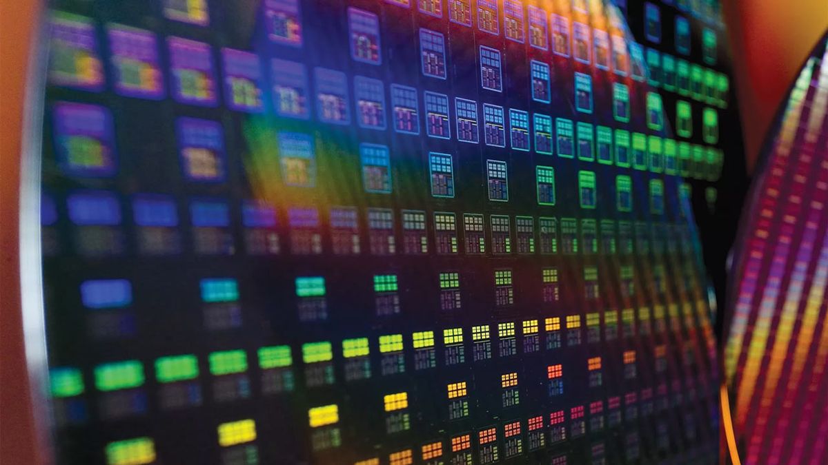

Now this does not paint the entire picture, since transistors are becoming more power efficient and there are other changes like chiplets and packaging that are leading to continued improvement, but these improvements are unlikely to push semiconductor technology further at historic rates.

I think there are two major implications here. The first is around the discussion on weather or not China can catch up on semiconductor manufacturing. I would argue that they may not need to in order to be successful. If they can drive down costs at 7nm and make their own packaging innovations, they can probably compete on a cost/performance basis in many applications.

The second implication is around AI. To a very large degree the AI industry has relied on increases in computing power to drive forward advances using larger and more sophisticated models. See below:


The typical AI model size, which is highly related to the compute required to train and run the models, has increased by roughly 4 orders of magnitude in the last 10 years. Thats a factor of 10,000. This is all while the cost per transistor has been flat. Anecdotally I played quite a bit with deep learning models in 2014-2016, and I could train a state of the art deep learning model on my home lab, with had 2 high end Nvidia GPUs which together cost about $2000-$3000. From what I've heard, today's deep learning models require clusters of 100+ NVidia GPUs that cost around $30k each to train. Again this is anecdotal, but a state of the art model could be trained on $3000 of hardware 10 years ago, and now a state of the art model requires at least $3,000,000 in hardware. A factor of roughly 1000.

There has still been a substantial improvement in training costs/model parameter, but I suspect room for further improvement on that metric going to be limited, and AI companies have reached the point where I don't think they can rely on building bigger models with more parameters. I could certainly be wrong though.
 
There are companies/people who track wafer manufacturing costs. To me that is the most relevant data. Based on that you can figure out transistor costs. Let me see if I can get the latest numbers for N3 and maybe N2. Hopefully others can chime in here so I am not the only datapoint.

By the way, I know the author: Zvi Or-Bach, President & CEO, MonolithIC 3D Inc. Very smart guy but he is selling product here.
 
Would also be curious on the related claim that Pat Gelsinger made that High NA EUV may enable "cost scaling to continue". (i.e. implying 14A/10A might be cheaper per transistor than 18A?).
 
Would also be curious on the related claim that Pat Gelsinger made that High NA EUV may enable "cost scaling to continue". (i.e. implying 14A/10A might be cheaper per transistor than 18A?).
I doubt it, at more advanced nodes it seems like an ever increasing portion of the costs go to things like wafer cleaning, HVAC, and other supporting systems. The smaller you go the cleaner the wafer needs to be, cleaner the air needs to be, the more dampening you need, ect.
 
Would also be curious on the related claim that Pat Gelsinger made that High NA EUV may enable "cost scaling to continue". (i.e. implying 14A/10A might be cheaper per transistor than 18A?).
He should consider why the Low NA was not able to do so for going to smaller design rules.
 
Do we think that wafer costs will decline at 7nm, 5nm, and 3nm after fabs are mostly depreciated? If so, it may be that 3nm will be the sweet spot with the current process/manufacturing combo. If there are advantages to the huge AI chips that compensate for higher transistor cost, then the high end will continue to progress. Note: Intel’s internal wafer costs WILL go down after the fab is depreciated. They will have an advantage at the older nodes.
 
He should consider why the Low NA was not able to do so for going to smaller design rules.
Intel / Pat also claimed that Intel 4 / 3 improves their cost competitvness. 10nm is / was very expensive for Intel (quad patterning) and Intel 3 supposedly improves this, so low NA does enable scaling of per transistor cost (maybe even total wafer cost?). Imo, the issue was that at the time Intel was designing their 10nm, they did not really believe in EUV, so they designed it for DUV.

There are some hints that Intel 18A won't really scale MMP compared to Intel 3, which means that even for 18A process, Intel might be able to use single EUV patterning for all metal layers, which would be very sensible given their lack of money and EUV machines. This almost hints to Intel using very similar metal stack to what is used for Intel 3, except it's on the backside to enable density scaling.

As for 14A / 10A, semianalysis speculated that Intel is going to use direct selfassembly, which could mitigate some issues with high NA EUV (random defects, secondary electron damage), although, it brings other kinds of defects. https://semiengineering.com/directed-self-assembly-gets-another-look/
 
Last edited:
Intel / Pat also claimed that Intel 4 / 3 improves their cost competitvness. 10nm is / was very expensive for Intel (quad patterning) and Intel 3 supposedly improves this, so low NA does enable scaling of per transistor cost (maybe even total wafer cost?). Imo, the issue was that at the time Intel was designing their 10nm, they did not really believe in EUV, so they designed it for DUV.

There are some hints that Intel 18A won't really scale MMP compared to Intel 3, which means that even for 18A process, Intel might be able to use single EUV patterning for all metal layers, which would be very sensible given their lack of money and EUV machines. This almost hints to Intel using very similar metal stack to what is used for Intel 3, except it's on the backside to enable density scaling.

As for 14A / 10A, semianalysis speculated that Intel is going to use direct selfassembly, which could mitigate some issues with high NA EUV (random defects, secondary electron damage), although, it brings other kinds of defects. https://semiengineering.com/directed-self-assembly-gets-another-look/

Intel did not do EUV at 10/7nm for two reasons: First, EUV was years late and would not be ready in time if Intel hit their 10nm schedule, which they did not. Second was the world famous Intel hubris. Intel took a very big risk and lost while TSMC took the less risky path and won.

It is the tortoise and hare story all over again:

 
Intel / Pat also claimed that Intel 4 / 3 improves their cost competitvness. 10nm is / was very expensive for Intel (quad patterning) and Intel 3 supposedly improves this, so low NA does enable scaling of per transistor cost (maybe even total wafer cost?). Imo, the issue was that at the time Intel was designing their 10nm, they did not really believe in EUV, so they designed it for DUV.

There are some hints that Intel 18A won't really scale MMP compared to Intel 3, which means that even for 18A process, Intel might be able to use single EUV patterning for all metal layers, which would be very sensible given their lack of money and EUV machines. This almost hints to Intel using very similar metal stack to what is used for Intel 3, except it's on the backside to enable density scaling.

As for 14A / 10A, semianalysis speculated that Intel is going to use direct selfassembly, which could mitigate some issues with high NA EUV (random defects, secondary electron damage), although, it brings other kinds of defects. https://semiengineering.com/directed-self-assembly-gets-another-look/
From their 2022 investor meeting https://semiwiki.com/semiconductor-manufacturers/intel/308311-intel-2022-investor-meeting/ they showed this:
INTEL-EUV-UPDATE-FEBRUARY-2022-1920x1014.png

Why is 30 nm their pitch limit? It's not from NA.

If Intel 18A minimum metal pitch is below 30 nm, they would be using (going back to?) multipatterning. This seems a little like history repeating itself.
 
From their 2022 investor meeting...
Isn't 30nm approximate pitch limit for single exposure low NA EUV? I think it is. Going below will require EUV double patterning. TSMC 2nm will probably also require it, which is why it might be more expensive than 18A on pure wafer processing cost. Of course Intel has other issues that drive the cost up...
 
Isn't 30nm approximate pitch limit for single exposure low NA EUV? I think it is. Going below will require EUV double patterning. TSMC 2nm will probably also require it, which is why it might be more expensive than 18A on pure wafer processing cost. Of course Intel has other issues that drive the cost up...
You can go beyond 30 nm like 28 nm or 26 nm and get the same results with Low or High NA, since the images would be formed the same way.
Stochastics seems to be the concern at even larger pitches than 30 nm. So again, the NA wouldn't help. In fact, the higher NA requires thinner resist, which makes things worse.
I just checked the 2022 Intel 4 paper, the 30 nm pitch M0 was done by SAPQ instead of EUV direct print, so indeed it was excluded from the >30 nm pitch condition. At SPIE, they had also shown defects at 32 nm pitch. Other metal layers with larger pitches such as 45 nm were done with EUV, though in those cases, the DUV alternative would have been simpler pitch halving rather than quartering.

I'm sure they're still trying to do 30 nm pitch or a little lower with direct print. But it's really the stochastic situation that will determine if it's viable.
 
Last edited:
The economic data are very well aligned with the paper published here a couple years ago, "Moore's Law is Dead; Long-live the Chiplett." Keep in mind, Moore's Law was a purely economic statement / prediction; of course, based on the anticipated advances in fabrication technology.
 
The economic data are very well aligned with the paper published here a couple years ago, "Moore's Law is Dead; Long-live the Chiplett." Keep in mind, Moore's Law was a purely economic statement / prediction; of course, based on the anticipated advances in fabrication technology.
This was my starting reference, I’m looking at how things have evolved in the last 2-3 years since then and going forward and it seems like from a cost per transistor standpoint chips stopped getting cheaper after 28nm, but you were still getting better transistor performance at the same price on other measures like power efficiency.

I also suspect that the costs will increase at a faster rate than performance gains going forward

The paper referenced was written in a way to help people outside the industry understand the economic advances we all enjoyed during the run up to the dilemma we face today. As an insider who understands these advances, you might want to skip the first five or six pages. Beyond that though, I think you'll enjoy the data. The data suggest that it wasn't a flat cut at 28nm, but close enough to where we can use that as a tipping point. It also covers the fixed costs, which are important to consider along with the variable costs.

Naturally, higher volume designs (smart phone AP for example) distribute those fixed costs more favorably, so you have to do a little math. However, with variable costs rising, even slightly, the total cost per transistor is higher with advanced nodes, so there we now have to draw lines between higher costs and improved performance, and due to the central issue being defect density, we also have to think about what parts of a design are better (more economically) done in a chiplet processed on a trailing edge node. It gets complicated.

From 50K feet though, we should also consider the macro-economic implications. I think the benefits afforded by Moore's Law have been vastly underestimated in the equations of inflation and economic growth. Those advantages are not there going forward.

The paper is not a prediction that we've run smack into an impassable object - we haven't. There are other things outside advances described by Moore's Law like advances in software, architecture (AI) and in chiplet designs, and of course, improved performance at leading edge nodes that will be provide improved utility, open new end use opportunities and economic benefits.
 
Back
Top