Array
(
    [content] =>
    [params] => Array
        (
            [0] => /forum/threads/how-are-the-benefits-of-bspd-affected-by-3d-stacking.23416/
        )

    [addOns] => Array
        (
            [DL6/MLTP] => 13
            [Hampel/TimeZoneDebug] => 1000070
            [SV/ChangePostDate] => 2010200
            [SemiWiki/EmailDomainReplace] => 1000010
            [SemiWiki/Newsletter] => 1000010
            [SemiWiki/WPMenu] => 1000010
            [SemiWiki/XPressExtend] => 1000010
            [ThemeHouse/XLink] => 1000970
            [ThemeHouse/XPress] => 1010570
            [XF] => 2031070
            [XFI] => 1060170
        )

    [wordpress] => /var/www/html
)
Guests have limited access.
Join our community today!
Join our community today!
You are currently viewing SemiWiki as a guest which gives you limited access to the site. To view blog comments and experience other SemiWiki features you must be a registered member. Registration is fast, simple, and absolutely free so please, join our community today!
You are using an out of date browser. It may not display this or other websites correctly.
You should upgrade or use an alternative browser.
You should upgrade or use an alternative browser.
How are the benefits of BSPD affected by 3D stacking?
- Thread starter Xebec
- Start date
Are you asking about die-to-die stacking (face-to-face, face-to-back), chiplets in vertical integration, or high-bandwidth memory (HMB) stacked atop logic?
Xebec
Well-known member
"Yes"Are you asking about die-to-die stacking (face-to-face, face-to-back), chiplets in vertical integration, or high-bandwidth memory (HMB) stacked atop logic?
") But I'm most curious about 3D stacking of logic on top of logic. Do the benefits of BSPD decrease or perhaps increase vs. non-BSPD fabrication vs. non-stacked logic.
But I'm most curious about 3D stacking of logic on top of logic. Do the benefits of BSPD decrease or perhaps increase vs. non-BSPD fabrication vs. non-stacked logic.MKWVentures
Moderator
Great question. To make it simple. Are there issues with Stacking a regular DDR5 DRAM with TSV on top of a logic device with BSPD?
Intel has the first BSPD process at 18A. TSMC N2 does not have it. TSMC is scheduled to support BSPD at A16 in 2026/2027. Unfortunately the HPC market has not figured it out yet. Hopefully Intel products will use it and provide a proof point for the market to follow.
 semiwiki.com
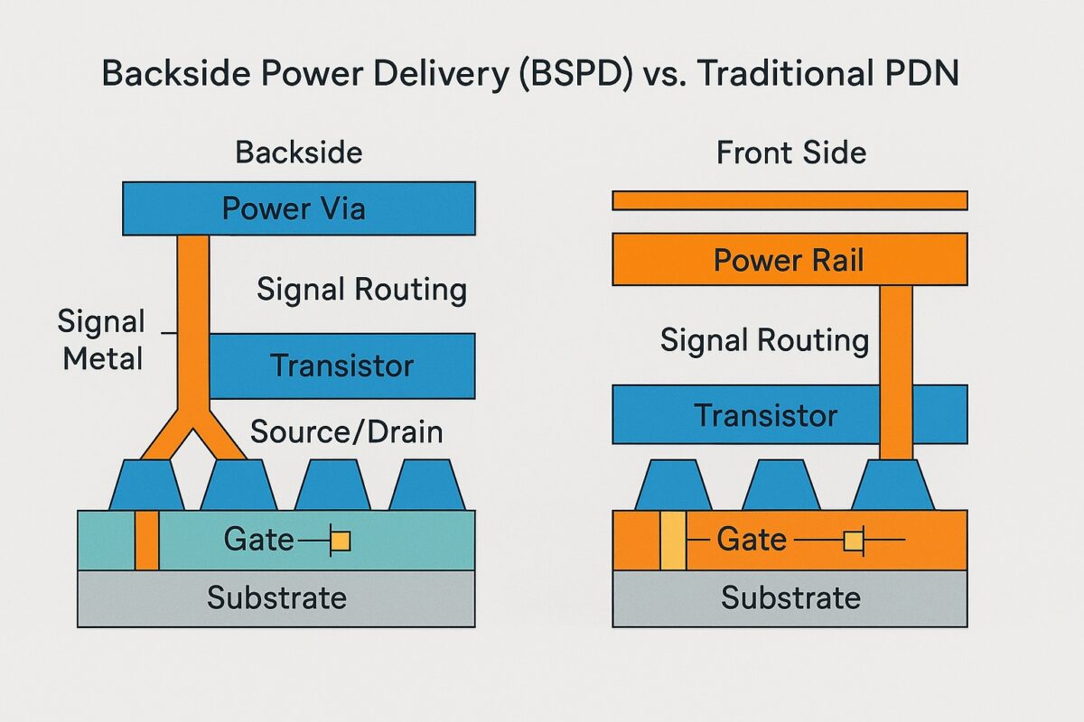
Backside Power Delivery (BSPD) Wiki - Semiwiki
Backside Power Delivery (BSPD), also called Backside Power Delivery Network (BSPDN) or backside power via (BPV) technology, is a semiconductor manufacturing innovation in which the chip’s primary power distribution network is relocated from the front side (transistor and signal interconnect...
Actually it improve the power delivery mechanism a lot with BSPD.
As wiki said, the benefits including
-Reduced IR Drop:
-Improved Power Efficiency:
-Better Power Integrity:.
-Freed Front-Side Routing:
-Enhanced 3D Integration Potential:
the first 3 items enhance the power delivery designs to provide excellent
power quality with less voltage drops and free from power delivery noises
such as ground/power bouncing noises, which will improve power integrity a lots,
especially for power hunger applications.
but for 3D integration, since there is more space for signal routing, so the micro bumps placement and route may be easier to design.
siliconbruh999
Well-known member
How do you get the heat out of BSPDN for desktop chips clocking 6+ GHz ?
Yes, since there is no real chip available for review the effects for BSPDN, we don't know for sure how it help for heat dispersion. But therapeutically speaking, since the IR drop on power network been reduced significantly, the waste heat should reduce dramatically. so heat issue should be easier to solve. By the way, since the power delivery traces should be on backside mostly, so the heat dispersion paths can be on both sides of the chip's surfaces.On the contrary, since the BSPDN can be wired separately from the signal wiring, isn't there a Merit in terms of exhaust heat, not a disadvantage?
Actually I'm not sure because there is no precedent for a chip that uses BSPDN
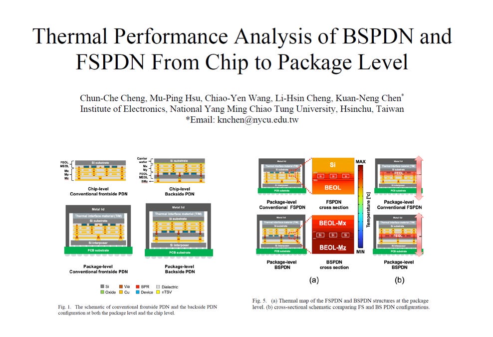
The Thermal Frontier of BSPDN: IITC 2025 Highlights from NYCU
Original Articles by SemiVision Research ( IEEE IITC , NYCU , TSMC )
 tspasemiconductor.substack.com
At the 2025 IEEE ECTC, TSMC unveiled several advanced thermal management solutions aimed at addressing the challenges posed by high power density chips. These include innovations in thermal interface materials (TIMs), package-level microchannel cooling, and thermal simulation analysis of SoIC structures. Building on this, the paper presented by Professor Kuan-Neng Chen’s team at IITC further sharpens the focus by tackling system-level thermal resistance modeling and thermal diffusion path planning under the BSPDN (Backside Power Delivery Network) architecture, offering a highly engineering-relevant perspective.
Why is this paper significant?
1. Deep technical insight:Unlike previous studies that approached BSPDN mainly from a conceptual or electrical optimization standpoint, this research concretely simulates the thermal resistance stack-up introduced by backside power delivery implementation. It highlights key challenges such as thermal bottlenecks in the BEOL, the reduced heat spreading efficiency after wafer thinning, and the vertical thermal resistance introduced by the integration of buried power rails (BPR) and nano-TSVs.
2. Cross-scale thermal analysis – from microscale to macroscale:
The study goes beyond chip-level microstructural thermal effects (e.g., in the BEOL and active layers) and extends into the package-level domain, examining thermal conduction behavior in elements such as interposers, underfill, and molding compounds. This results in a comprehensive chip-to-package thermal transfer model.
3. Identification of thermal “design bottlenecks”:
The results reveal that while BSPDN enhances power delivery efficiency and shortens current paths, it also shifts the main heat dissipation path from the frontside metal layers (used in traditional FSPDN) to the less favorable backside. This architectural change introduces thermal bottlenecks, making it more difficult to direct heat flow efficiently toward cooling components—posing a critical risk in the design of future high-power AI accelerators and HPC chips.
4. Bridging advanced process technology and system-level engineering:
The paper also emphasizes that addressing the thermal challenges of BSPDN requires holistic design efforts—spanning materials science, wafer-level process engineering, EDA tool development, and packaging integration. This underscores that thermal design has become an integral and inseparable part of next-generation chip development.
Last edited:
Xebec
Well-known member
I would assume heat dissipation would be slightly improved. The area on top of the CPU becomes thinner - meaning less insulative material before you get to the die surface / heat spreader. I would think this would offset the increase in "under insulation" since the majority of heat goes out the top of the silicon (where the cooler is located).How do you get the heat out of BSPDN for desktop chips clocking 6+ GHz ?
(The metal layers on top - whether signal only or also including power, are encased in an insulative material).
That doesn't stack up with actual calculations/simulations I did when looking into BSPD.I would assume heat dissipation would be slightly improved. The area on top of the CPU becomes thinner - meaning less insulative material before you get to the die surface / heat spreader. I would think this would offset the increase in "under insulation" since the majority of heat goes out the top of the silicon (where the cooler is located).
(The metal layers on top - whether signal only or also including power, are encased in an insulative material).
With conventional FSPD the transistors sit right on the silicon substrate, which is a pretty good thermal conductor (about 50% compared to solid copper) -- the primary heat path (more than 90%) is through this substrate to the backside of the die, then through the TIM to the heatsink. Even a normal thickness substrate (e.g. 700um) has very low thermal resistance. There's also very good lateral thermal conduction to spread out the heat from circuit hotspots.
With BSPD the substrate is below the transistors on the I/O bump face of the die, with the thick metal and bumps below this; above the transistors are all the thin fine pitch metal layers (poor conductivity, low metal density with poor vertical connections) embedded in dielectrics (very low thermal conductivity, typically 100x worse than silicon) -- there's not even any thick metal with fat stacked vias which might help get heat out, these are all on the backside of the die below the transistors.
The fact that these topside metal/dielectric layers are relatively thin helps with vertical heat flow (but this is still a lot worse than silicon), but a particular problems is that the horizontal heat spreading at transistor level is also very poor since there's almost no silicon there. This really hits high-power-density structures such as clock drivers and high-speed SERDES, you get terrible hot-spots where the local transistor/metal temperature is *much* hotter than the heatsink and surrounding circuits. In one example I looked at, the worst local hotspots were +20C for FSPD and +50C for BSPD... :-(
This is one reason why TSMC currently recommend BSPD only for "actively-cooled" applications like (liquid-cooled?) HPC, where the heatsink can be kept pretty cool (e.g. 60C) so even with the worse hotspots you can still keep the transistors and fine-pitch metal within Tmax limits. There's no chance to run the heatsink at "normal" temperatures (e.g. 90C) encountered in many air-cooled applications.
Xebec
Well-known member
Very interesting. Just to make sure I get this - on silicon dies today, the primary heat path goes under and around rather than through the top of the transistors and metal layers above that?That doesn't stack up with actual calculations/simulations I did when looking into BSPD.
With conventional FSPD the transistors sit right on the silicon substrate, which is a pretty good thermal conductor (about 50% compared to solid copper) -- the primary heat path (more than 90%) is through this substrate to the backside of the die, then through the TIM to the heatsink. Even a normal thickness substrate (e.g. 700um) has very low thermal resistance. There's also very good lateral thermal conduction to spread out the heat from circuit hotspots.
With BSPD the substrate is below the transistors on the I/O bump face of the die, with the thick metal and bumps below this; above the transistors are all the thin fine pitch metal layers (poor conductivity, low metal density with poor vertical connections) embedded in dielectrics (very low thermal conductivity, typically 100x worse than silicon) -- there's not even any thick metal with fat stacked vias which might help get heat out, these are all on the backside of the die below the transistors.
The fact that these topside metal/dielectric layers are relatively thin helps with vertical heat flow (but this is still a lot worse than silicon), but a particular problems is that the horizontal heat spreading at transistor level is also very poor since there's almost no silicon there. This really hits high-power-density structures such as clock drivers and high-speed SERDES, you get terrible hot-spots where the local transistor/metal temperature is *much* hotter than the heatsink and surrounding circuits. In one example I looked at, the worst local hotspots were +20C for FSPD and +50C for BSPD... :-(
This is one reason why TSMC currently recommend BSPD only for "actively-cooled" applications like (liquid-cooled?) HPC, where the heatsink can be kept pretty cool (e.g. 60C) so even with the worse hotspots you can still keep the transistors and fine-pitch metal within Tmax limits. There's no chance to run the heatsink at "normal" temperatures (e.g. 90C) encountered in many air-cooled applications.
Is that why the "flipped die" around the Pentium II/III era was a big deal for cooling?
Can they add a 3D "conductive" layer in between the silicon die and either top side or bottom side (with electrical conductors poking through appropriately) to address this?
Thanks for correcting me here!
Correct, with conventional FSPD almost all heat (typically >90%) goes from the transistors down into the silicon substrate underneath (or on top with a flip-chip) and then through the TIM between the die backside and the heatsink/package lid. The silicon substrate acts as an excellent heat-spreader for small hot circuits, like are found in high-speed SERDES or clock drivers.Very interesting. Just to make sure I get this - on silicon dies today, the primary heat path goes under and around rather than through the top of the transistors and metal layers above that?
Is that why the "flipped die" around the Pentium II/III era was a big deal for cooling?
Can they add a 3D "conductive" layer in between the silicon die and either top side or bottom side (with electrical conductors poking through appropriately) to address this?
Thanks for correcting me here!
You can't add an "extra layer" because the chip is in the way -- and with BSPD it's the bits that are poor thermal conductors, thin metal/vias and dielectrics on the frontside. Even if you bonded more silicon on top of this, the heat still has to wriggle its way from the transistor through these layers to get to it. If you put a TIM in the way instead (relatively poor conductivity, quite thick) this makes the heat-spreading problem even worse -- it's OK at the back of a thick silicon substrate, it's terrible right above the frontside layers.
This is not a minor theoretical problem, it's a major stumbling block for chips with ultra-high-speed circuits (very high power density in a small area) where liquid cooling is not possible (or the heatsink is not cold enough, which is the same thing). We can't even consider using BSPD processes until a solution is found... :-(
Last edited:
That said, BSPDN also has different methods.Correct, with conventional FSPD almost all heat (typically >90%) goes from the transistors down into the silicon substrate underneath (or on top with a flip-chip) and then through the TIM between the die backside and the heatsink/package lid. The silicon substrate acts as an excellent heat-spreader for small hot circuits, like are found in high-speed SERDES or clock drivers.
You can't add an "extra layer" because the chip is in the way -- and with BSPD it's the bits that are poor thermal conductors, thin metal/vias and dielectrics on the frontside. Even if you bonded more silicon on top of this, the heat still has to wriggle its way from the transistor through these layers to get to it. If you put a TIM in the way instead (relatively poor conductivity, quite thick) this makes the heat-spreading problem even worse -- it's OK at the back of a thick silicon substrate, it's terrible right above the frontside layers.
This is not a minor theoretical problem, it's a major stumbling block for chips with ultra-high-speed circuits (very high power density in a small area) where liquid cooling is not possible (or the heatsink is not cold enough, which is the same thing). We can't even consider using BSPD processes until a solution is found... :-(
It may be solved if the design or layout that actually uses it is refined.
At least if you're trying to introduce it, Intel may have prepared some kind of plan.
Like I said, how big a problem this is depends on the chip design. There's a fundamental thermal problem with BSPD if you have small circuits on-chip with high power density, I gave a couple of examples. If you can spread out/distribute the "hot bits" (or keep the heatsink cooler) then BSPD is less of a problem, you just end up with all the transistors running a bit hotter.That said, BSPDN also has different methods.
It may be solved if the design or layout that actually uses it is refined.
At least if you're trying to introduce it, Intel may have prepared some kind of plan.
There's no "magic sauce" here, it's basic physics -- thin/narrow metal layers with tiny vias all surrounded by dielectric on the frontside are lousy at heat conduction, both vertical and lateral. If you try and put in big slabs of metal/multiple via pillars on the frontside to help then you've just reintroduced what you tried to get rid of by moving power distribution to the backside, the density goes back down and you've lost one of the big advantages of BSPD (moving all this heavy metal to underneath the transistors).
Maybe this is OK for Intel with relatively low clock rates (*only* 6GHz!) and large functional blocks. It's definitely not OK at 10x the clock rate... :-(
Like I said, this is based on actual circuit thermal simulations, not marketing handwaving and Powerpoint publicity slides... ;-)
BSPD is garbage... It's a pityLike I said, how big a problem this is depends on the chip design. There's a fundamental thermal problem with BSPD if you have small circuits on-chip with high power density, I gave a couple of examples. If you can spread out/distribute the "hot bits" (or keep the heatsink cooler) then BSPD is less of a problem, you just end up with all the transistors running a bit hotter.
There's no "magic sauce" here, it's basic physics -- thin/narrow metal layers with tiny vias all surrounded by dielectric on the frontside are lousy at heat conduction, both vertical and lateral. If you try and put in big slabs of metal/multiple via pillars on the frontside to help then you've just reintroduced what you tried to get rid of by moving power distribution to the backside, the density goes back down and you've lost one of the big advantages of BSPD (moving all this heavy metal to underneath the transistors).
Maybe this is OK for Intel with relatively low clock rates (*only* 6GHz!) and large functional blocks. It's definitely not OK at 10x the clock rate... :-(
Like I said, this is based on actual circuit thermal simulations, not marketing handwaving and Powerpoint publicity slides... ;-)
With this, Intel's process will also be a piece of crap