Array
(
    [content] => 
    [params] => Array
        (
            [0] => /forum/threads/rapidus-achieves-significant-milestone-at-its-state-of-the-art-foundry-with-prototyping-of-leading-edge-2nm-gaa-transistors.23208/
        )

    [addOns] => Array
        (
            [DL6/MLTP] => 13
            [Hampel/TimeZoneDebug] => 1000070
            [SV/ChangePostDate] => 2010200
            [SemiWiki/Newsletter] => 1000010
            [SemiWiki/WPMenu] => 1000010
            [SemiWiki/XPressExtend] => 1000010
            [ThemeHouse/XLink] => 1000970
            [ThemeHouse/XPress] => 1010570
            [XF] => 2021770
            [XFI] => 1050270
        )

    [wordpress] => /var/www/html
)

Rapidus Achieves Significant Milestone at its State-of-the-Art Foundry with Prototyping of Leading-Edge 2nm GAA Transistors

Daniel Nenni

Admin
Staff member

First prototypes successfully demonstrate electrical characteristics as the company continues to hit targets leading up to 2027 mass-production​


TOKYO, July 18, 2025—Rapidus Corporation, a manufacturer of advanced logic semiconductors, today announced that prototyping has started for its 2nm gate-all-around (GAA) transistor structure at Rapidus’ Innovative Integration for Manufacturing (IIM-1) foundry. The prototype wafers also started to obtain their electrical characteristics.

Rapidus’ new IIM-1 foundry represents a significant advancement over the traditional foundry model. The company is re-imagining how semiconductor factories should think, learn, adapt and optimize processes in real time through cutting-edge methods and technology including:

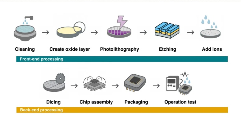
  • Fully single-wafer front-end processing: In a single-wafer process, adjustments can be made to a single wafer, inspected and if successful, applied to all subsequent wafers. Single wafer captures more data, enabling AI models to be trained to improve wafer production and increase yields. Rapidus is one of the first companies that will commercialize fully single-wafer processing, which is central to its Rapid and Unified Manufacturing Service (RUMs).

  • Extreme Ultraviolet (EUV) lithography: EUV lithography is one of the key technologies for realizing 2nm semiconductors. An advanced lithography process is critical for forming the 2nm generation GAA structure. Rapidus is the first company to install advanced EUV machinery in Japan. Additionally on April 1, 2025, the company successfully completed EUV exposure, approximately three months after the equipment was delivered in December 2024.
In less than three years, Rapidus has achieved its IIM-1 target milestones – from initial groundbreaking in September 2023, clean room completion in 2024 and, in June 2025, the connection of more than 200 of the world’s most advanced pieces of semiconductor equipment. These achievements are complemented by today’s announcement of prototyping of 2nm GAA transistors and attaining electrical characteristics.

Rapidus is developing a Process Development Kit compatible with IIM-1’s 2nm process and will release it to advance customers by Q1 2026, while preparing an environment in which customers can start their own prototypes. Rapidus will begin mass-production in 2027.

Rapidus-Wafer-Photo-1024x683.jpg
Prototypes of 2nm Gate All Around Transistors on Silicon Wafer

About Rapidus Corporation
Rapidus Corporation aims to develop and manufacture the world’s most advanced logic semiconductors. We will create new industries together with our customers through the development and provision of services to shorten cycle times in design, wafer processes, 3D packaging, and more. We will continue to challenge ourselves in order to contribute to the fulfillment, prosperity and happiness of people’s lives through the use of semiconductors.

About Rapidus Corporation
Headquarters: 4-1 Kojimachi, Chiyoda-ku, Tokyo 102-0032, Japan
Establishment:August 10th, 2022
Executives:Tetsuro Higashi, Chairman of the Board of Directors
Atsuyoshi Koike, President and Representative Director
Business:Research, development, design, manufacture, and sales of semiconductor devices, integrated circuits and other electronic components
Capital, etc:7,346 million yen (as of November 2022)
(includes the amount of capital reserve)

U.S. Media Contact:
Breakaway Communications for Rapidus
Email: rapidus@breakawaycom.com
 
One thing I can tell you is that Rapidus is investing HEAVILY in the ecosystem. They will outrun Intel 18A and Samsung 2F in regards to commercial IP by the end of the year, absolutely. Of course, all IP is developed on TSMC first then ported over. In contrast to Samsung Foundry where you have to have a customer signed up before IP is made available which is a time-to-market delay.


One thing I can tell you is that Rapidus is investing HEAVILY in the ecosystem. They will outrun Intel 18A and Samsung 2F in regards to commercial IP by the end of the year, absolutely. Of course, all IP is developed on TSMC first then ported over. In contrast to Samsung Foundry where you have to have a customer signed up before IP is made available which is a time-to-market delay.
great for the eco-system IP folks selling picks and shovels.
 
One thing I can tell you is that Rapidus is investing HEAVILY in the ecosystem. They will outrun Intel 18A and Samsung 2F in regards to commercial IP by the end of the year, absolutely. Of course, all IP is developed on TSMC first then ported over. In contrast to Samsung Foundry where you have to have a customer signed up before IP is made available which is a time-to-market delay.


This is lightning fast progress, from groundbreaking to wafer prototyping, especially when compared to a new US fab project. By the way, what does it exactly mean when they say, “The prototype wafers also started to obtain their electrical characteristics”? Is it a reasonable milestone or too basic?
 
This is lightning fast progress, from groundbreaking to wafer prototyping, especially when compared to a new US fab project. By the way, what does it exactly mean when they say, “The prototype wafers also started to obtain their electrical characteristics”? Is it a reasonable milestone or too basic?
I am surprised they have made it this far. But to see if a technology works, I want to see a SRAM test chip data and details on entire process and the cross section showing layers .

Saying "electrical characteristics" sounds like a transistor test chip and Ring oscillator. Intel and TSMC have CFETS with these.

If @Daniel Nenni says IP companies and customers are working with them ..... that is a big deal.... they must be further along than I ever expected.

Broadcom is running test chips with no big red flags thus far. Toyota, Sony, Denso, Kioxia, and NEC are investors so they are probably doing test chips as well. The close partnership with big customers is the key to the foundry business. Intel Foundry had better get some big customers to help them with 14A or I fear all will be lost.

I'm as shocked as anyone about the progress. IBM is not a great process development partner in my experience. HVM yield has always been a challenge. Rapidus wafer capacity is supposed to be 10k+ WPM in 2027 and 50k+ by the end of 2028 so there is not a lot of wafers available anytime soon. Rapidus seems to have an advantage on the NOT TSMC N2 market however. Being the newcomer is better than failing on the previous 2 nodes. :LOL:

Meanwhile TSMC N3 is 1M+ WPM and N2 will be a fast follower. TSMC said they are moving N5 capacity to N3 yet N3 capacity is still tight. Crazy, and N2 has more design starts than N3!?!?!?
 
Back
Top