Exactly, I use the Intel Core i5-13500, i5-13600K, and i7-14700K myself. The i5-13600K offers a good balance of performance and power consumption. The i5-13500 operates at significantly lower power. If you pair any of these CPUs with a Z790 motherboard and DDR4 memory, the overall system cost can be quite reasonable.This is not true tbh unless you are buying top of the line like I7/I9 and a 13600K is relatively less power hungry good and has a decent price tag no need for exotic Ram as well the platform is cheaper as well (Z690/790) somethings are just made up you can also buy 12600K/12700K for cheap as well
Array
(
    [content] =>
    [params] => Array
        (
            [0] => /forum/threads/christmas-season-cpu-best-sellers-rank-on-amazon-amd-vs-intel.21739/page-2
        )

    [addOns] => Array
        (
            [DL6/MLTP] => 13
            [Hampel/TimeZoneDebug] => 1000070
            [SV/ChangePostDate] => 2010200
            [SemiWiki/Newsletter] => 1000010
            [SemiWiki/WPMenu] => 1000010
            [SemiWiki/XPressExtend] => 1000010
            [ThemeHouse/XLink] => 1000970
            [ThemeHouse/XPress] => 1010570
            [XF] => 2031070
            [XFI] => 1060170
        )

    [wordpress] => /var/www/html
)
Guests have limited access.
Join our community today!
Join our community today!
You are currently viewing SemiWiki as a guest which gives you limited access to the site. To view blog comments and experience other SemiWiki features you must be a registered member. Registration is fast, simple, and absolutely free so please, join our community today!
You are using an out of date browser. It may not display this or other websites correctly.
You should upgrade or use an alternative browser.
You should upgrade or use an alternative browser.
Christmas Season CPU Best Sellers Rank on Amazon: AMD vs. Intel
- Thread starter hist78
- Start date
MKWVentures
Moderator
So its like 3 12th gen, 1 13th Gen, 1 14th Gen from Intel??Yes, the OEM market is different and influenced by the factors I mentioned earlier. My question is, why is Intel performing so poorly in Amazon retail sales? Especially considering there are no Intel CPUs in the top 10 Amazon Best Sellers rankings for Amazon US. From expensive to budget models, AMD is performing exceptionally well. Is this due to performance, price-to-performance ratio, or something else? If this trend spills over into the OEM market, Intel could face even bigger trouble.
As of December 25, 2024:
View attachment 2597
AMD is dominating right now and it will dominate in the near future. With upcoming GPU generation that will be unveiled in january both from AMD and Nvidia the performance needs will again increase thus X3D CPU sales will be very high.

Desktop PCs - Worldwide | Statista Market Forecast
Worldwide: The revenue generated in the Desktop PCs market worldwide in **** amounts to US$*****bn. Definition: Desktop PCs are personal computing devices designed for stationary use, typically placed on a desk or workstation.
 www.statista.com
I don't really understand what you mean by this statistics.Desktop PCs - Worldwide | Statista Market Forecast
Worldwide: The revenue generated in the Desktop PCs market worldwide in **** amounts to US$*****bn. Definition: Desktop PCs are personal computing devices designed for stationary use, typically placed on a desk or workstation.
The desktop market is very limited. Personally, I think resources should be redirected to other areas, such as low-power devices that can compete with Apple's and Qualcomm's offerings—for example, Lunar Lake and Panther Lake. For desktops, GPUs are also important, and the Intel B580 is a step in the right direction. Additionally, Intel could enhance its lineup by including more capable NPUs with improved software support for AI.I don't really understand what you mean by this statistics.
The desktop CPU market is limited but AMD can still grow a lot in that are eating away at Intel's market share. Basically X3D chips are what will be the best seller for some time especially due to the need for stronger cpu's again.The desktop market is very limited. Personally, I think resources should be redirected to other areas, such as low-power devices that can compete with Apple's and Qualcomm's offerings—for example, Lunar Lake and Panther Lake. For desktops, GPUs are also important, and the Intel B580 is a step in the right direction. Additionally, Intel could enhance its lineup by including more capable NPUs with improved software support for AI.
Xebec
Well-known member
Would like a short discussion here as I've heard this from a lot of places too. I've asked around here about "is cost per transistor still decreasing for new nodes", and the answer is always yes (though not as quickly as it used to).Additionally, Arrow Lake is produced on a more expensive node (N3B) than Zen 5 (N4) and is sold at a higher price.
Is it really true that N3B is "more expensive" than N4? I agree a 100mm2 product on both nodes would cost more on N3B, but as N3B is denser - you're getting more transistors per mm2. This should mean a "cheaper" node if the products have equal capability/transistor count (+ other benefits such as improved perf/watt).
Given the size of the DIY desktop market, I don't think it will significantly impact AMD's share price. For AMD, it needs to demonstrate its ability to compete with Nvidia in the AI market. For Intel, it needs to showcase competitive products on the 18A process, stabilize its server CPU market share, and introduce competitive AI accelerators.The desktop CPU market is limited but AMD can still grow a lot in that are eating away at Intel's market share. Basically X3D chips are what will be the best seller for some time especially due to the need for stronger cpu's again.
It seems to me that the other big problem in server cpu's is that the margins for Intel myst be pretty low for Intel cause AMD'S making more money now in that area despite having lower market share.Given the size of the DIY desktop market, I don't think it will significantly impact AMD's share price. For AMD, it needs to demonstrate its ability to compete with Nvidia in the AI market. For Intel, it needs to showcase competitive products on the 18A process, stabilize its server CPU market share, and introduce competitive AI accelerators.
MKWVentures
Moderator
@Jumper @XYang2023
Intel sells about 2-2.5x more desktop CPUs than AMD. This despite the fact that desktop is not a priority. So while AMD is eating share, it is not dominant anywhere
Server is similar but the challenge for Intel on server is that server IS the priority and Intel is still losing share. This is just on CPUs. AMD revenue is about 10x Intel on DC GPUs
So Datacenter is the priority for Intel on both CPU and GPU and everything else. The DC CPU market moves slow so Clearwater forest will have no material impact on Intel revenue in 2025 (<$500M in sales in 2025). Intel will most likely lose share or maybe hold the line on DC CPU in 2025.
It has to do with the kinds of customer that builds a PC. They are tech oriented, and value minded. Many are gamers.Yes, the OEM market is different and influenced by the factors I mentioned earlier. My question is, why is Intel performing so poorly in Amazon retail sales? Especially considering there are no Intel CPUs in the top 10 Amazon Best Sellers rankings for Amazon US. From expensive to budget models, AMD is performing exceptionally well. Is this due to performance, price-to-performance ratio, or something else? If this trend spills over into the OEM market, Intel could face even bigger trouble.
As of December 25, 2024:
View attachment 2597
AMD dominates this small market due to their value, gaming performance, and dedication to a long term platform support. Intel seems to switch their socket and mb requirements every couple of years. This practice does not lend itself to an inexpensive performance upgrade in the future.
I think that this tiny market is so small, and so very different to the main consumer of x86 products that it is largely irrelevant. Just my opinion.
Thanks for giving me the opportunity to do some math homework!Would like a short discussion here as I've heard this from a lot of places too. I've asked around here about "is cost per transistor still decreasing for new nodes", and the answer is always yes (though not as quickly as it used to).
Is it really true that N3B is "more expensive" than N4? I agree a 100mm2 product on both nodes would cost more on N3B, but as N3B is denser - you're getting more transistors per mm2. This should mean a "cheaper" node if the products have equal capability/transistor count (+ other benefits such as improved perf/watt).

While the cost per transistor decreases with process advancements, fabless companies often prefer to pack more transistors into their designs to boost performance. If the transistor count remains the same with a new node, the cost savings benefit the fabless company rather than the end users. This doesn't provide much incentive for end users. A good example is Apple's SoC for iPhone, where die sizes have consistently been around 100 ± 15 mm² in recent years.
Now, let's compare Arrow Lake and Zen 5 using their top models.
The compute tile of the Core Ultra 9 285K (Arrow Lake-S) is 114.5 mm². The 8-core CCD of Zen 5 is 70.6 mm², and the 9900X/9950X models require two CCDs, totaling 141.2 mm².
141.2 / 114.5 = 1.233, meaning Zen 5 uses 23.3% more area for its top model compared to Arrow Lake.
The next question is cost, which is tricky to estimate. It's unclear which N4 node Zen 5 uses—N4, N4P, N4X, or even N4C (a cheaper version of N4P).
According to some reports, the price of N3 is 25% higher than N5. Considering N4 is close to N5 and has seen cost reductions over the years, we can assume the cheaper process cost for Zen 5 can offset the 23.3% larger area.
Additionally, AMD likely enjoys better loyalty discounts from TSMC than Intel. The smaller CCD die (70.6 mm² on N4 vs. 114.5 mm² on N3B) on a more mature node also brings yield benefits, translating to lower costs.
References:
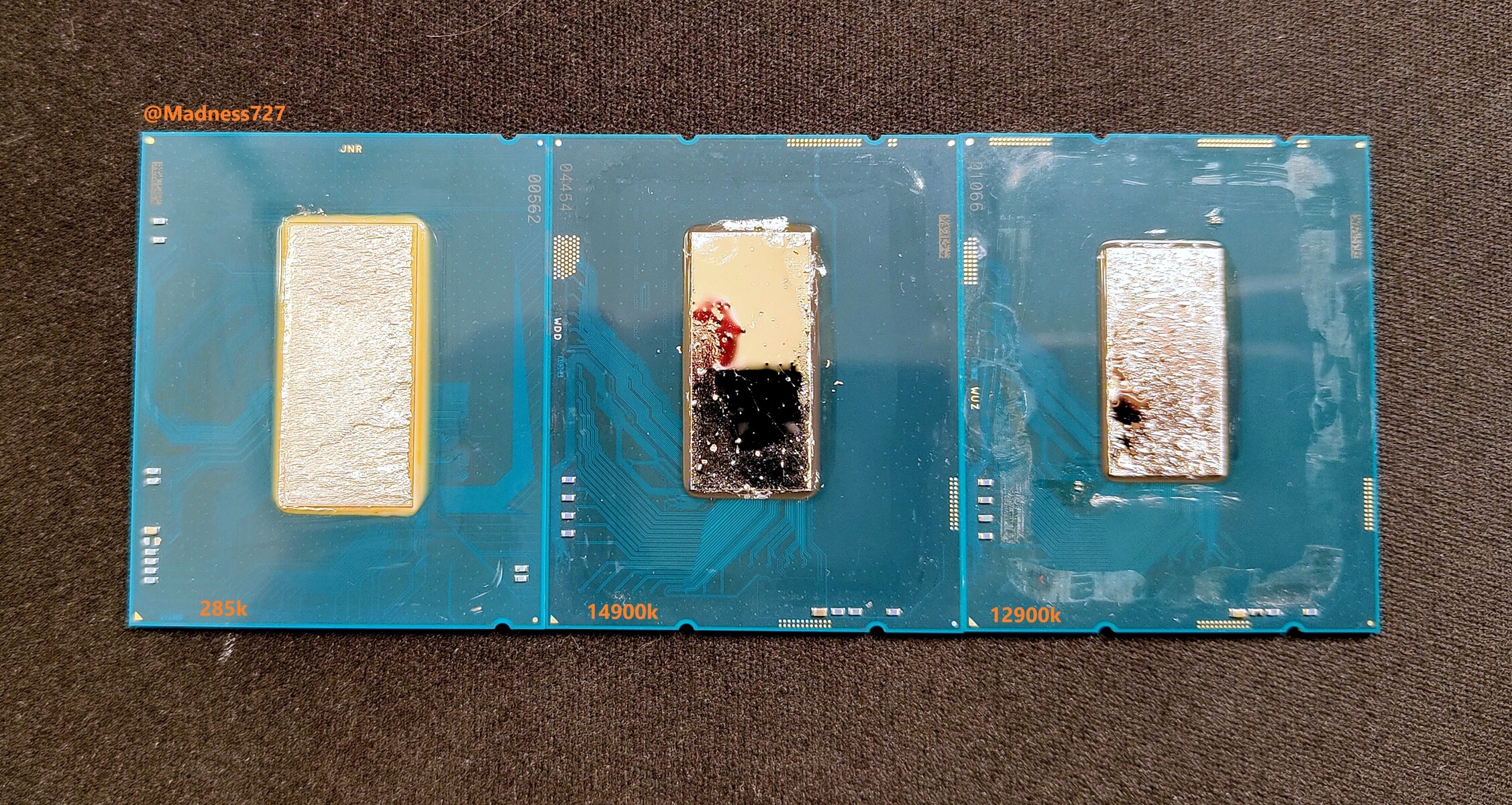
Intel Arrow Lake-S Die Visibly Larger Than Raptor Lake-S, Die-size Estimated
As a quick follow-up to last week's "Arrow Lake-S" de-lidding by Madness727, we now have a line-up of a de-lidded Core Ultra 9 285K "Arrow Lake-S" processor placed next to a Core i9-14900K "Raptor Lake-S," and the Core i9-12900K "Alder Lake-S." The tile-based "Arrow Lake-S" is visibly larger...
www.techpowerup.com

AMD Granite Ridge and Strix Point Zen 5 Die-sizes and Transistor Counts Confirmed
AMD is about give the new "Zen 5" microarchitecture a near-simultaneous launch across both its client segments—desktop and mobile. The desktop front is held by the Ryzen 9000 "Granite Ridge" Socket AM5 processors; while Ryzen AI 300 "Strix Point" powers the company's crucial effort to capture...
www.techpowerup.com
... and there is the real issue for Intel (not Amazon sales of desktop processors).@Jumper @XYang2023
Intel sells about 2-2.5x more desktop CPUs than AMD. This despite the fact that desktop is not a priority. So while AMD is eating share, it is not dominant anywhere
Server is similar but the challenge for Intel on server is that server IS the priority and Intel is still losing share. This is just on CPUs. AMD revenue is about 10x Intel on DC GPUs
So Datacenter is the priority for Intel on both CPU and GPU and everything else. The DC CPU market moves slow so Clearwater forest will have no material impact on Intel revenue in 2025 (<$500M in sales in 2025). Intel will most likely lose share or maybe hold the line on DC CPU in 2025.
AMD got out ahead of Intel with designs that were architected to scale from thin and light to high core count DC products. They spent time getting chiplets working very well, and designed a very good working IOD with plenty of bandwidth to feed tons of cores.
For the past several years, AMD has totally dominated Intel in DC. Even the new Granite Rapids release with Intel pulling out all the stops still lags AMD's Turin by an average of 40% and is priced higher. At least Intel is no longer being trounced by triple digit performance deficits!
I also worry a little about Clearwater Forest. The Darkmont core is supposed to be a "slightly modified Skymont" core. From what I can see, that means it will not have SMT as I believe that this would require a pretty significant overhaul of the entire core to implement.
At this time, it looks like Skymont is about on-par with Zen 4 in terms of IPC.... as long as you don't throw MT at it, or AVX512. Since it is silly to talk about anything other than MT with DC products, Zen 5c will have a roughly 40% performance per clock (vs instructions per clock) advantage over the current Skymont core due to SMT.
Between SMT and AVX512 .... and Zen 5c's current performance on N3E for Turin, I do wonder if an entire product based on Darkmont (E cores) can hang with Turin Dense in DC workloads.
Is Clearwater Forest supposed to also compete with Turin (non D) and its full Zen 5 cores?
Anyway, this is where I think the real fight for dominance in x86 from a profit standpoint will be.
It seems to me that the other big problem in server cpu's is that the margins for Intel myst be pretty low for Intel cause AMD'S making more money now in that area despite having lower market share.
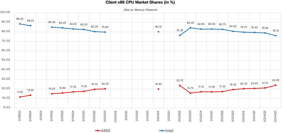
The server CPU segment is where Intel is experiencing significant losses. According to Mercury Research's data:Server is similar but the challenge for Intel on server is that server IS the priority and Intel is still losing share. This is just on CPUs. AMD revenue is about 10x Intel on DC GPUs
So Datacenter is the priority for Intel on both CPU and GPU and everything else. The DC CPU market moves slow so Clearwater forest will have no material impact on Intel revenue in 2025 (<$500M in sales in 2025). Intel will most likely lose share or maybe hold the line on DC CPU in 2025.
In Q3 2024, AMD's unit market share was 24.2%, while its revenue share was 33.9%, which is notably higher than its unit share.
If we calculate further: Intel's unit market share is 75.8% (100% - 24.2%), and its revenue share is 66.1% (100% - 33.9%).
The average selling price (ASP) for AMD's server CPU products compared to Intel's is: (33.9%/24.2%) / (66.1%/75.8%) = 1.606.
This means AMD's ASP is 60% higher than Intel's. Essentially, AMD is selling more high-end models to capture premium prices, while Intel is focusing on mid-to-low-end products to maintain market share.
AMD's desktop PC market share skyrockets amid Intel's Raptor Lake CPU crashing scandal — AMD makes biggest leap in recent history
Though Intel says it was an inventory adjustment at one of its customers.
I can never get a good read on price per wafer at TSMC as different sources change over time and don't seem to include enough data across enough nodes; however, the trend line is more than linear, it is exponential (but not severely so).Thanks for giving me the opportunity to do some math homework!
While the cost per transistor decreases with process advancements, fabless companies often prefer to pack more transistors into their designs to boost performance. If the transistor count remains the same with a new node, the cost savings benefit the fabless company rather than the end users. This doesn't provide much incentive for end users. A good example is Apple's SoC for iPhone, where die sizes have consistently been around 100 ± 15 mm² in recent years.
Now, let's compare Arrow Lake and Zen 5 using their top models.
The compute tile of the Core Ultra 9 285K (Arrow Lake-S) is 114.5 mm². The 8-core CCD of Zen 5 is 70.6 mm², and the 9900X/9950X models require two CCDs, totaling 141.2 mm².
141.2 / 114.5 = 1.233, meaning Zen 5 uses 23.3% more area for its top model compared to Arrow Lake.
The next question is cost, which is tricky to estimate. It's unclear which N4 node Zen 5 uses—N4, N4P, N4X, or even N4C (a cheaper version of N4P).
According to some reports, the price of N3 is 25% higher than N5. Considering N4 is close to N5 and has seen cost reductions over the years, we can assume the cheaper process cost for Zen 5 can offset the 23.3% larger area.
Additionally, AMD likely enjoys better loyalty discounts from TSMC than Intel. The smaller CCD die (70.6 mm² on N4 vs. 114.5 mm² on N3B) on a more mature node also brings yield benefits, translating to lower costs.
References:
Intel Arrow Lake-S Die Visibly Larger Than Raptor Lake-S, Die-size Estimated
As a quick follow-up to last week's "Arrow Lake-S" de-lidding by Madness727, we now have a line-up of a de-lidded Core Ultra 9 285K "Arrow Lake-S" processor placed next to a Core i9-14900K "Raptor Lake-S," and the Core i9-12900K "Alder Lake-S." The tile-based "Arrow Lake-S" is visibly larger...www.techpowerup.comAMD Granite Ridge and Strix Point Zen 5 Die-sizes and Transistor Counts Confirmed
AMD is about give the new "Zen 5" microarchitecture a near-simultaneous launch across both its client segments—desktop and mobile. The desktop front is held by the Ryzen 9000 "Granite Ridge" Socket AM5 processors; while Ryzen AI 300 "Strix Point" powers the company's crucial effort to capture...www.techpowerup.com
As you point out, Zen 5 does currently use 23.3% more die area for its top model; however, Arrow Lake loses to Zen 5 in MT in aggregate by a good margin.
In DC applications, where margins and profit are very high, I don't see how Intel's architecture in Skymont (lacking SMT and AVX512) can hope to compete with Zen 5 cores. Additionally, once you shrink Zen 5 to N3E and compare it to Skymont (not all of Arrow Lake), things look more favorable for Zen 5 ..... and Zen 5 includes SMT and AVX512.
Of course, the great hope for Intel is that the current latency issues they have with tiles will be overcome in Clearwater Forest and that with some tweaks, Skymont (Darkmont) will increase in performance well.
Still, being an engineer for so many decades, I always come back to the old adage: "You don't get something for nothing".
If Intel can't recover the high profit DC market, they have a serious issue IMO. I am pulling for a successful Clearwater forest on 18A.
From what I can see, Both Sierra Forest and Granite Rapids are significantly behind in DC workload testing:
Both Sierra Forests and Granite Rapids are alright in terms of performance. Also Granite Rapids supports MRDIMM which can have noticeable impacts with LLM applications.
x.com
x.com
This is the deficit that Clearwater forest has to erase. As I said earlier, at least Intel is no longer losing by tripple digit numbers in these tasks as it was; however, Intel prices are significantly higher than Turin the last time I looked. Not sure I would want to be an Intel DC salesman at this time. How to you pitch a higher cost, lower performance, lower efficiency product?
Clearwater forest may well help clean this up; however, as pointed out, I don't see this helping Intel financially in 2025.
And then there is the AMD Zen 6 which looks to be released around Early to mid 2026 with its reported 32 core CCD's (Desktop I think is rumored to be only 12 core CCD's). 384 core single socket anyone?
Intel needs a home run with Clearwater forest IMO.... or a bailout by the US government (or both).
Intel's current objective is to keep pace with AMD and then work to regain market share with more competitive products, such as Clearwater and Diamond Rapids. MJ confirmed this in a recent conference. This scenario is likely unfavorable for AMD.From what I can see, Both Sierra Forest and Granite Rapids are significantly behind in DC workload testing:
This is the deficit that Clearwater forest has to erase. As I said earlier, at least Intel is no longer losing by tripple digit numbers in these tasks as it was; however, Intel prices are significantly higher than Turin the last time I looked. Not sure I would want to be an Intel DC salesman at this time. How to you pitch a higher cost, lower performance, lower efficiency product?
Clearwater forest may well help clean this up; however, as pointed out, I don't see this helping Intel financially in 2025.
And then there is the AMD Zen 6 which looks to be released around Early to mid 2026 with its reported 32 core CCD's (Desktop I think is rumored to be only 12 core CCD's). 384 core single socket anyone?
Intel needs a home run with Clearwater forest IMO.... or a bailout by the US government (or both).
It doesn't need bailout. At worst case, sellout Altera and Mobileye holdings to repay debt and further delaying Ohio fabs. It also doesn't need a home run. It needs to keep up with competition and recover its financial condition. If just value Intel products alone, it should be more valuable than AMD. Its valuation is shaded by the manufacturing business.