Samsung, 1a DRAM redesign in jeopardy… HBM competitiveness recovery 'super strong'
[Samsung DRAM's Tasks abc ①] Developing Countermeasures to HBM Sluggishness… Outlines to be Outlined by the End of the YearSemiconductor/Display Input: 2024/10/15 16:55 Modified: 2024/10/16 14:38
Reporter Jang Kyung-yoon
The crisis surrounding Samsung Electronics is raising its head again. The source of the crisis seems to be largely centered on semiconductors. Among them, the recovery of memory competitiveness centered on the HBM business and the sluggish foundry are being pointed out. The rebuilding of the organizational culture of trust and communication is also key. Accordingly, ZDNet Korea will examine the fundamental problems of the Samsung crisis theory and seek opportunities for a leap forward together. [Editor's Note]
Samsung Electronics is in crisis. All of its business divisions, including semiconductors, home appliances, MX, and SDC, are struggling, but it is especially painful that its main business, memory, failed to shine even in the boom cycle of the third quarter of this year.
Among them, the market’s disappointment in the HBM (high bandwidth memory) business was great. Samsung Electronics had been working behind the scenes to start supplying HBM3E to Nvidia in earnest from the third quarter of this year. However, it has not yet passed the quality test for the 8-layer product, and there is a high possibility that the 12-layer product will be delayed until the second or third quarter of next year.
There are complex reasons for Samsung Electronics' delay in commercializing HBM. However, experts point out that the fundamental problem with HBM is the problem of the core die, DRAM. In the HBM structure where multiple DRAMs are stacked vertically and connected, the performance of DRAM is inevitably directly linked to the performance of HBM.
EUV preemptive application, but… 1a DRAM competitiveness shaken
From this perspective, the point at which Samsung Electronics' position as number one in DRAM technology was greatly shaken is pointed out to be the '1a DRAM'.
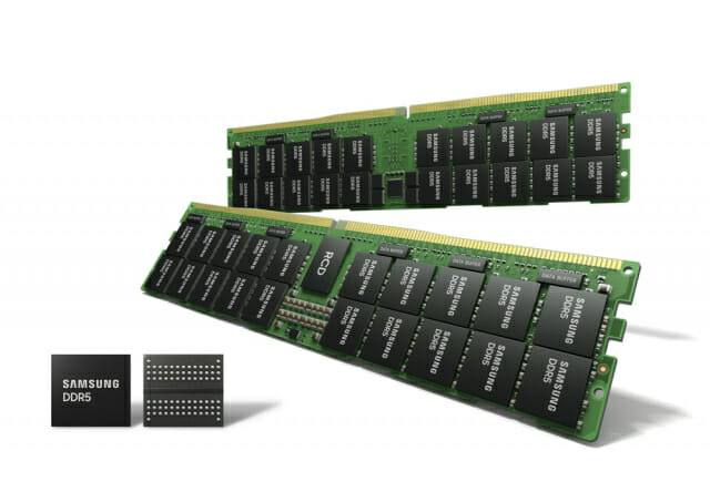
10nm-class DRAM has evolved in the order of 1x (1st generation) - 1y (2nd generation) - 1z (3rd generation) - 1a (4th generation) - 1b (5th generation). 1a DRAM has a line width of 14 nanometers (nm). Samsung Electronics began mass production in the second half of 2021.
Samsung Electronics was unable to mass-produce 1a DRAMs faster than its competitors, but it sought to increase its competitiveness by more actively introducing cutting-edge technologies such as EUV (extreme ultraviolet lithography). The number of EUV layers applied by Samsung Electronics to 1a DRAMs was 5, which was more than that of its competitor SK Hynix (1).
However, the prevailing opinion is that such attempts have not led to successful results as of now. EUV is advantageous in miniaturizing line widths compared to ArF (argon fluoride), the existing exposure process (the process of engraving circuits on semiconductors). Therefore, the advantage of EUV is that it can increase process efficiency and reduce manufacturing costs, which are the core of memory.
However, EUV has high technical difficulty, which has been a factor in reducing process stability during actual mass production. As a result, the cost of Samsung Electronics' 1a DRAM did not decrease as initially expected.
The DRAM design itself is also evaluated as not being perfect. In particular, it is known that the development of server products was delayed compared to competitors due to setbacks. In fact, SK Hynix was the first to receive certification for server DDR5 products based on 1a DRAM from Intel in January of last year.
Discussion of ‘redesign’ amid delay in HBM commercialization… Attempt at a major transformation
There are also claims that the performance of 1a DRAM is holding back Samsung Electronics' recent sluggish mass production of HBM3E for Nvidia.
Recently, Samsung Electronics conducted a field test with NVIDIA on the HBM3E 8-stage product at the Pyeongtaek campus. NVIDIA concluded the field test itself without any particular issues. However, it is known that they evaluated that the data processing speed of HBM is lower than that of other products.
According to a comprehensive analysis of the stories inside and outside of Samsung Electronics, Samsung Electronics’ HBM3E 8-stage data processing speed (Gbps) is about 10% lower than that of SK Hynix and Micron. The specific figures vary depending on test results and customers, but there is no disagreement that the performance is lacking compared to the two competitors that use 1b DRAM.
Accordingly, Samsung Electronics is considering a 'super-strong' measure to restore the fundamental competitiveness of server DRAM and HBM under the leadership of Vice Chairman Jeon Young-hyun.
In a recent apology following the announcement of the provisional third quarter results, the former vice chairman stated, “Above all, I will restore our fundamental technological competitiveness,” and “Technology and quality are our lifeblood and Samsung Electronics’ pride that we can never compromise on.” He also said, “Rather than short-term solutions, I will secure fundamental competitiveness,” and “Furthermore, I believe that the only way for Samsung Electronics to make a comeback is through new technologies that have never existed in the world and perfect quality competitiveness.”
According to multiple sources familiar with the matter, Samsung Electronics has recently been internally discussing a plan to redesign some of the circuitry of its 1a DRAM.
An industry insider explained, "Samsung Electronics, which is struggling with its memory strategy, has concluded that it needs to redesign its 1a DRAM," adding, "However, the final decision has not been made, and it is a situation where bold decisions are needed because it will require taking on many risks."
삼성, 1a D램 재설계 고심…HBM 경쟁력 회복 '초강수' 두나
삼성전자가 위기를 맞았다. 반도체를 비롯해 가전, MX, SDC 등 전 사업부가 난항을 겪고 있지만, 주력 사업인 메모리 분야가 올 3분기 호황 사이클에서도 빛을 발하지 못했다는 점이 특히 뼈아프다.그 중에서도 HBM(고대역폭메모리) 사업에 대한 시장의 실망감은 컸다. 삼성전자는 당초 엔비...