You are currently viewing SemiWiki as a guest which gives you limited access to the site. To view blog comments and experience other SemiWiki features you must be a registered member. Registration is fast, simple, and absolutely free so please, join our community today!
DÜSSELDORF. The chip manufacturer Globalfoundries wants to expand its factory in Dresden: capacity is to be almost doubled by the end of the decade. The US group will invest eight billion dollars for this, said CEO Thomas Caulfield to the Handelsblatt on the sidelines of a customer event in Munich.
The manager is demanding government support to the same extent as that received by rival TSMC for its planned plant in Dresden. For the Taiwanese, the state covers half of the costs. That means: Caulfield calculates subsidies of four billion dollars.
Federal government circles confirm that Globalfoundries has made representations to the Federal Ministry of Economics and the Chancellery and has expressed its desire for government support. However, Berlin has not yet taken a concrete position.
The semiconductor money grab continues. I attended an event at the GF Dresden Fab years ago and wondered why Angela Merkel did not get behind GF's expansion efforts. She was at the event. I guess GF was ahead of their time. To bad it took a deadly pandemic to get proper semiconductor awareness.
Germany seems focused on automotive so my guess would be CMOS, AMS, RF, etc... GF already has FDSOI in Dresden. They have a lot of land so a giga fab is possible. GF has the Samsung 14nm so it could be that as well. I'm wondering when Samsung get's into the EU fab building mix. They have (3) fabs in Korea and (2) in the US.
And when are memory makers going to globalize? You can't have logic without memory, right?
They do up to 12LPP, but I don't think they do FDX stuff (could be wrong on this though) as I think that is at Malta. The ancient stuff is all at Singapore because that was the Chartered part of the business whereas Malta/Dresden was AMD.
They do up to 12LPP, but I don't think they do FDX stuff (could be wrong on this though) as I think that is at Malta. The ancient stuff is all at Singapore because that was the Chartered part of the business whereas Malta/Dresden was AMD.
Is GF allowed to build FinFET (14/12) outside of the US? Any insight difficulty of reproducing that recipe?
On memory, I speculate that GF is likely focused on coming up with a single chip DUV solution, utilizing MRAM, ReRAM, of some other of these higher density NVM without the backside connections (Ian said no on that). Getting that to work is a big deal.
The semiconductor money grab continues. I attended an event at the GF Dresden Fab years ago and wondered why Angela Merkel did not get behind GF's expansion efforts. She was at the event. I guess GF was ahead of their time. To bad it took a deadly pandemic to get proper semiconductor awareness.
Germany seems focused on automotive so my guess would be CMOS, AMS, RF, etc... GF already has FDSOI in Dresden. They have a lot of land so a giga fab is possible. GF has the Samsung 14nm so it could be that as well. I'm wondering when Samsung get's into the EU fab building mix. They have (3) fabs in Korea and (2) in the US.
And when are memory makers going to globalize? You can't have logic without memory, right?
When German, Japanese, and US government consider the amount and percentage to subsidize a fab project, in addition to those typical economical and political factors, they have to evaluate the future prospects of the technology and product that particular semiconductor company can keep bringing into the countries.
For GlobalFoundries, its major technology development stopped at 7nm in 2018. What's the future picture can GlobalFoundries draw for the German government?
But for the Intel, TSMC, and Samsung, they can bring lots of possibilities (or dreams) about the leading edge technologies and future upgrade into the discussion even they might not implement it in Germany, Japan, or US right away.
They can tell the German government 14nm is 3x the speed for the same and a lot less leakage than 28nm with a recipe that they should have mastered by now. NXP is making chips based on TSMC 16nm in 2025.
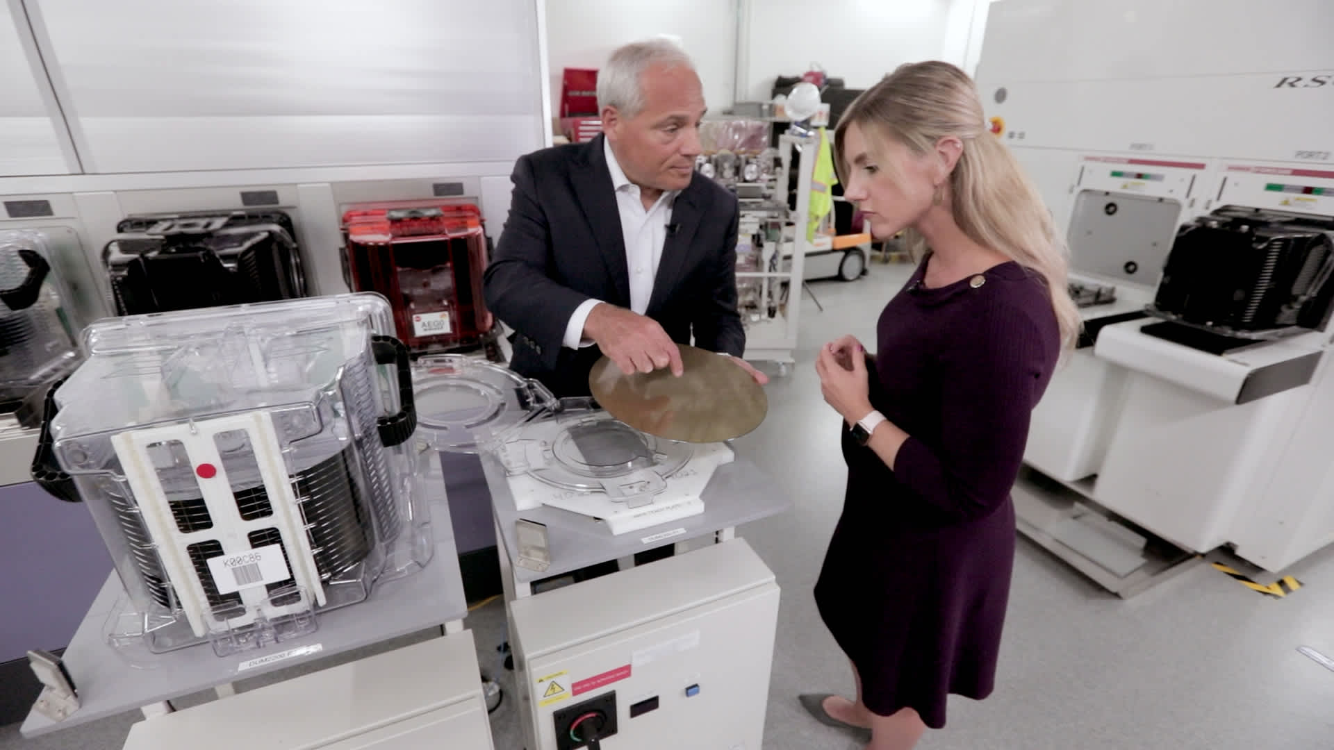
GlobalFoundries is manufacturing more of the world's critical chips, gaining significance with U.S.-China tension and big deals like one with General Motors
Mr Blue, do you disagree with this strategy "To this day, GlobalFoundries only makes 12-nanometer chips and above, or what it calls 'essential' chips.")? Some of us neanderthals do. Also, they operate from a good political location. He and Gunslinger operate from good strategic locations and should theoretically succeed. What do you think?
Do you like Caulfield's and Gunslinger's strategy?
Does anybody have any opinions on execution (yield and employee efficiency for example)?
I'm not expert enough in the fabrication industry overall to judge GF's essential chip strategy. That said, it seems a bit weird to fab lower cost chips in high cost countries, unless GF is assuming long-term subsidies.
I agree with Gelsinger's strategy to bet big on IFS. As I've posted before, I think the merchant datacenter chip market overall is in decline in marketshare, so being a fab is where the future is. In-house designs are a rising wave with cloud datacenter companies. But IFS is a very long way from being viable enough to support Intel as a whole, or even to be a big contributor, so it's a risky strategy. I'll admit, I find Gelsinger's cheerleading demeanor to be tiresome. Beyond Gelsinger's IFS strategy, I'm not seeing much from Intel I'm impressed with, product-wise or leadership-wise.
DÜSSELDORF. The chip manufacturer Globalfoundries wants to expand its factory in Dresden: capacity is to be almost doubled by the end of the decade. The US group will invest eight billion dollars for this, said CEO Thomas Caulfield to the Handelsblatt on the sidelines of a customer event in Munich.
The manager is demanding government support to the same extent as that received by rival TSMC for its planned plant in Dresden. For the Taiwanese, the state covers half of the costs. That means: Caulfield calculates subsidies of four billion dollars.
Federal government circles confirm that Globalfoundries has made representations to the Federal Ministry of Economics and the Chancellery and has expressed its desire for government support. However, Berlin has not yet taken a concrete position.
GlobalFoundries is manufacturing more of the world's critical chips, gaining significance with U.S.-China tension and big deals like one with General Motors
I saw Tom at the GF foundry event last month. Great guy, I have known him for years. Very smart, but I'm surprised GF is not using IBM process technologies. IBM is developing leading edge technology that GF could manufacture? A lot of the GF people are former IBM including Tom, and now IBM is taking their leading edge technology to Japan (Rapidus)?
GF will succeed with what they have but what are the long term expansion plans? New fabs and new process nodes are coming fast and furious all over the world. We will have an over supply then what? Packaging is becoming the new foundry battleground, how will GF compete?
Compete with what? What's wrong with trying to dominate at the edge, with local gadgets, with mixed signal, and lots of add-ons? If foreign goods are blocked or tariffed... If the DoD needs a secured foundry, If the countries want to continue to print money and pay for this... it seems like 22/12nm FDSOI and 14nm poly with fins seem like a good play to me. I suspect they will expand with exotic memory. IMO, charging for faster throughput would be a good play.
Packaging can be left to Skywater and packaging companies. Why does a foundry need to do that?
I like the strategy. The execution isn't historically very good. Things change.
I saw Tom at the GF foundry event last month. Great guy, I have known him for years. Very smart, but I'm surprised GF is not using IBM process technologies. IBM is developing leading edge technology that GF could manufacture? A lot of the GF people are former IBM including Tom, and now IBM is taking their leading edge technology to Japan (Rapidus)?
GF will succeed with what they have but what are the long term expansion plans? New fabs and new process nodes are coming fast and furious all over the world. We will have an over supply then what? Packaging is becoming the new foundry battleground, how will GF compete?
Very smart, but I'm surprised GF is not using IBM process technologies. IBM is developing leading edge technology that GF could manufacture? A lot of the GF people are former IBM including Tom, and now IBM is taking their leading edge technology to Japan (Rapidus)?
I mean they kind of did. The issue seemed to just be scale. If they couldn't even fill malta (which is like about 1-2 TSMC phases in size from the looks of pictures) while only being 1 year later than TSMC, how on earth would they ramp a 2LPP hard enough to make the economics work out. Even with AMD and IBM for initial ramps GF was subscale and had slow ramps. Without them I don't know how they even get yields and cost to a good spot for second wave or trailing customers even if we ignore the lack of scale/R&D amortization.
GF will succeed with what they have but what are the long term expansion plans? New fabs and new process nodes are coming fast and furious all over the world. We will have an over supply then what? Packaging is becoming the new foundry battleground, how will GF compete?
Maybe tight collaboration with OSATs against their common enemy of COWS/INFLO is the best strategy if TSMC doesn't want to play ball with other foundries outside of supporting UCIE? Either way for the markets GF plays in, I wouldn't be surprised if TSMC, intel, and Samsung's adv packaging tech never catches on outside of niche use cases' like Cliff's where unit cost are of lower importance.
14nm poly with fins seem like a good play to me. I suspect they will expand with exotic memory. IMO, charging for faster throughput would be a good play.
I know you hate "foundry units" Cliff, so I must unfortunately be the bearer of bad news. GF 14LPP has a poly of 78nm. 12FDX being 84nm. Also my understanding was that 12FDX was still planar rather than finFET. Regardless 12FDX is a fascinating from an intellectual perspective with how much blood they are squeezing from the planar stone (22FDX isn't too shabby in this respect either). I wish GF and it's customers would just ramp the node already so I can dig into some teardowns. My understanding is this would also be their first from the ground up node to reach HVM since like 32HP.
I mean they kind of did. The issue seemed to just be scale. If they couldn't even fill malta (which is like about 1-2 TSMC phases in size from the looks of pictures) while only being 1 year later than TSMC, how on earth would they ramp a 2LPP hard enough to make the economics work out. Even with AMD and IBM for initial ramps GF was subscale and had slow ramps. Without them I don't know how they even get yields and cost to a good spot for second wave or trailing customers even if we ignore the lack of scale/R&D amortization.
Maybe tight collaboration with OSATs against their common enemy of COWS/INFLO is the best strategy if TSMC doesn't want to play ball with other foundries outside of supporting UCIE? Either way for the markets GF plays in, I wouldn't be surprised if TSMC, intel, and Samsung's adv packaging tech never catches on outside of niche use cases' like Cliff's where unit cost are of lower importance.
I know you hate "foundry units" Cliff, so I must unfortunately be the bearer of bad news. GF 14LPP has a poly of 78nm. 12FDX being 84nm. Also my understanding was that 12FDX was still planar rather than finFET. Regardless 12FDX is a fascinating from an intellectual perspective with how much blood they are squeezing from the planar stone (22FDX isn't too shabby in this respect either). I wish GF and it's customers would just ramp the node already so I can dig into some teardowns. My understanding is this would also be their first from the ground up node to reach HVM since like 32HP.
It is a competitive moat as well as being an excellent selling point to get folks on the train in the first place.
12FDX has been on the cards for many years but has never made it into production, presumably because the added double-patterning complexity over 22FDX increases cost considerably but without much improvement in PPA -- customers wanting high-density digital will go to FinFET at 7nm and below because the density is higher than 12FDX and cost per gate is lower, customers wanting the "special features" (and IP libraries) of 22FDX don't see a strong reason to move to 12FDX.
Mr. Ng, you are quoting the poly pitch, not the length of the poly, although the gate pitch is not a bad way of specifying a process.
Ian, good insight. I have been hearing about the 12nm FDSOI, but I have never received a DRM from it. Then again, I didn't push too hard for it either. 22nm gate length on that process is probably good enough. I think the MRAM and ReRAM may be the more interesting additions to that process.
 view.redaktion.handelsblatt.com