Array
(
    [content] => 
    [params] => Array
        (
            [0] => /forum/threads/more-than-moore-ibm-announces-0-7nm-process-node-significant-logic-sram-scaling-vs-2nm.25369/
        )

    [addOns] => Array
        (
            [DL6/MLTP] => 13
            [Hampel/TimeZoneDebug] => 1000070
            [SV/ChangePostDate] => 2010200
            [SemiWiki/EmailDomainReplace] => 1000010
            [SemiWiki/Newsletter] => 1000010
            [SemiWiki/WPMenu] => 1000010
            [SemiWiki/XPressExtend] => 1000010
            [ThemeHouse/XLink] => 1000970
            [ThemeHouse/XPress] => 1010570
            [XF] => 2031070
            [XFI] => 1060170
        )

    [wordpress] => /var/www/html
)

More than Moore - IBM Announces 0.7nm Process Node (Significant logic/SRAM scaling vs 2nm)

Xebec

Well-known member
A great article from Ian Cuttress -- partial take-aways to not spoil the full article:

- "When it comes to IBM, I firmly believe they’re in the camp of saying Moore’s Law is still alive."
- There are multiple types of CFET design in the literature, and specifically IBM has built a staggered sequential CFET design
- [Compared to IBM's 2nm - 40% SRAM scaling, 50% Logic scaling, more info in article]
- IBM is getting a High-NA machine..

The article also contrasts the major chip foundries approaches to future transistor types with what IBM is doing/planning, using plenty of charts and diagrams.

 
The really interesting bit is not just the PMOS/NMOS staggering but the fact that the NMOS and PMOS are on separately processed wafers which are cut on different crystal planes (<110> for PMOS, <001> for NMOS) to optimise the performance of each.

The key to all this is the new (proprietary?) "device-scale" wafer bonding process which IBM claim to have got working -- how this transfers to mass production remains to be seen, presumably any foundry which wanted to adopt the process will have to license this, and the differently-cut wafers, and the staggering.

All put together this offers some pretty compelling advantages, so it'll be interesting to see what the foundries (especially TSMC) do, adopt/license the IBM approach or try and come up with something of their own with similar advantages... :-)
 
This is interesting research. I congratulate my friends at IBM for research and their leadership

But IBM does not manufacture semiconductors for itself or anyone else. Correct?

IBM 2nm was "announced" over 5 years ago and it is still 2+ years from anyone (Rapidus) using it in a real product that people buy.

So its an idea for conference attendees to discuss (Like university papers). It would seem it is unlikely to ever impact what actually happens in the industry

great comprehenive article by Ian...... I wish my brain could create, hold, and summarize that much information. Well done.
Didn't IBM do nanosheets before anyone else? And everyone has adopted them now... ;-)
 
If you talk to IBM people, yes.

... and they invented wafers, GPUs, CMOS, cellphones, grand theft auto,..... and wait for it ..... the question mark. :ROFLMAO::LOL::ROFLMAO::LOL:
Surely the point about IBM is that they're great at coming up with radical new technologies, but not necessarily ones that can easily be turned into a real high-yield cost-competitive mass-production process (directly or via licensing)?

This has happened in the the past with foundries who tried to do this and came unstuck (e.g. Samsung? STM?), maybe because IBM don't think hard enough about production/alignment margins -- so long as they get one working lot and can publish a paper about it (and license it?) that's their job done.

Still doesn't mean they didn't do it first (and deserve credit for that), or that it won't end up being widely adopted -- but often the foundry that succeeds is one that builds on the fundamental IBM idea but then does it better for mass production (e.g. TSMC...)

There are several major new ideas here which together give a pretty big PPA advantage, the question is whether they'll make it to MP (and when) and in which foundry.
 
The really interesting bit is not just the PMOS/NMOS staggering but the fact that the NMOS and PMOS are on separately processed wafers which are cut on different crystal planes (<110> for PMOS, <001> for NMOS) to optimise the performance of each.

The key to all this is the new (proprietary?) "device-scale" wafer bonding process which IBM claim to have got working -- how this transfers to mass production remains to be seen, presumably any foundry which wanted to adopt the process will have to license this, and the differently-cut wafers, and the staggering.

All put together this offers some pretty compelling advantages, so it'll be interesting to see what the foundries (especially TSMC) do, adopt/license the IBM approach or try and come up with something of their own with similar advantages... :-)
One of these IBM news releases is generating a lot of confusion. AFAIK, no one is able to bond two device wafers, one with PMOS and one with NMOS transistors, to generate a CFET at a 0.7nm-node pitch. The bond pitch would have to be < 50nm, which is not feasible.

Rather, what they are doing is to start with a device wafer (say, PMOS), then bond to it an unpatterned crystalline silicon film from a donor wafer (with a suitable bonding interface), and continue patterning this film to create the second device. This is what's called the "sequential CFET" process.
 
Last edited:
Surely the point about IBM is that they're great at coming up with radical new technologies, but not necessarily ones that can easily be turned into a real high-yield cost-competitive mass-production process (directly or via licensing)?

This has happened in the the past with foundries who tried to do this and came unstuck (e.g. Samsung? STM?), maybe because IBM don't think hard enough about production/alignment margins -- so long as they get one working lot and can publish a paper about it (and license it?) that's their job done.

Still doesn't mean they didn't do it first (and deserve credit for that), or that it won't end up being widely adopted -- but often the foundry that succeeds is one that builds on the fundamental IBM idea but then does it better for mass production (e.g. TSMC...)

There are several major new ideas here which together give a pretty big PPA advantage, the question is whether they'll make it to MP (and when) and in which foundry.
As you mentioned, It is well known that transfering a technology from IBM leads to severe problems. Intel also has a history of leading edge, high cost, unmanufacturable technologies.

As far are people using IBMs ideas, yes manufacturing companies look at all the research data from universities, IMEC, IBM, etc. I dont know of any technology in the last 15 years where a semicompany used IBM as a major input. They did invent the CMP technology we used in 1993.... But not Finfet, GAA, strained silicon,.... they did get a bunch of people to use Gate first HKMG LOL

But if people want to say IBM invented 2nm GAA because they did a ton of presentations, that is fine. We can talk if it is used in products that we can all buy someday.
 
Surely the point about IBM is that they're great at coming up with radical new technologies, but not necessarily ones that can easily be turned into a real high-yield cost-competitive mass-production process (directly or via licensing)?

This has happened in the the past with foundries who tried to do this and came unstuck (e.g. Samsung? STM?), maybe because IBM don't think hard enough about production/alignment margins -- so long as they get one working lot and can publish a paper about it (and license it?) that's their job done.

Still doesn't mean they didn't do it first (and deserve credit for that), or that it won't end up being widely adopted -- but often the foundry that succeeds is one that builds on the fundamental IBM idea but then does it better for mass production (e.g. TSMC...)

There are several major new ideas here which together give a pretty big PPA advantage, the question is whether they'll make it to MP (and when) and in which foundry.
If you talk to IBM people, yes.

... and they invented wafers, GPUs, CMOS, cellphones, grand theft auto,..... and wait for it ..... the question mark. :ROFLMAO::LOL::ROFLMAO::LOL:

IBM Semiconductor Technology Research (STR) is part of IBM Research and is in an awkward position. After IBM paid $1.5 billion to have GlobalFoundries take over its semiconductor manufacturing division in 2015, IBM became a semiconductor company that has labs but no fabs. IBM no longer has its own commercial fabs to test or co‑develop manufacturing technologies, let alone support high volume production.

Compared with the not‑for‑profit structures of IMEC in Belgium and ITRI in Taiwan, IBM STR operates under a for‑profit corporate umbrella and must keep producing leading edge, high visibility breakthroughs to justify its existence and attract new funding sources. This is challenging because there are only four leading edge semiconductor manufacturers in the world (excluding mainland China): three established incumbents - TSMC, Intel, and Samsung - and one potential newcomer, Japan’s Rapidus. Rapidus is the only company licensed to use IBM’s 2nm technology. TSMC, Samsung, and Intel all appear uninterested in adopting or paying for IBM’s technologies.

GlobalFoundries exited leading edge logic manufacturing in 2018. Worse, the deteriorating relationship between IBM and GlobalFoundries eventually led to lawsuits accusing each other of contract breaches or trade secret misappropriation. They finally settled these disputes in January 2025.

As leading edge semiconductor research and manufacturing become extremely expensive and complex, it is unclear how long the current business model and organizational scale of IBM Semiconductor Technology Research can remain sustainable.
 
IBM Semiconductor Technology Research (STR) is part of IBM Research and is in an awkward position. After IBM paid $1.5 billion to have GlobalFoundries take over its semiconductor manufacturing division in 2015, IBM became a semiconductor company that has labs but no fabs. IBM no longer has its own commercial fabs to test or co‑develop manufacturing technologies, let alone support high volume production.


As leading edge semiconductor research and manufacturing become extremely expensive and complex, it is unclear how long the current business model and organizational scale of IBM Semiconductor Technology Research can remain sustainable.
Since you mentiioned financials

1) IBM does its research lab acvitivies at Albany nanotech, correct? which is owned by the state and leased space to IBM? IBM does not own it?
2) tool are provided by other partners there for research, Does the state own those tools or does ASML etc.
3) Does IBM get paid to be there or pay to use the site? does Intel or Micron or samsung use this site?

Who pays IBM for IBM process research? not GF or Intel..... Do they have any partners other than Rapidus? or is it just government grants

thanks!
 
One of these IBM news releases is generating a lot of confusion. AFAIK, no one is able to bond two device wafers, one with PMOS and one with NMOS transistors, to generate a CFET at a 0.7nm-node pitch. The bond pitch would have to be < 50nm, which is not feasible.

Rather, what they are doing is to start with a device wafer (say, PMOS), then bond to it an unpatterned crystalline silicon film from a donor wafer (with a suitable bonding interface), and continue patterning this film to create the second device. This is what's called the "sequential CFET" process.
That doesn't seem to be what is described, unless I'm missing something -- otherwise you'd hit the usual thermal process budget problems with stacked devices, which they specifically say they avoid...
 
That doesn't seem to be what is described, unless I'm missing something -- otherwise you'd hit the usual thermal process budget problems with stacked devices, which they specifically say they avoid...
What's new in IBM's nanostack is that the stacked transistors are offset laterally, which gives better electrical access to the bottom device from the top. But otherwise, it's just a traditional sequential CFET process similar to what's been demonstrated by Imec and Intel. So they still have to deal with those thermal budget issues specific to the sequential process, although they may have made progress there. The article by Ian Cuttress summarizes the flow (my comments in italics):
  • - Build PFETs on carrier wafer with (110) channel
  • - Use 2nd carrier wafer to bond on the top layers of silicon with (001) channel <-- bonding of unpatterned Si/SiGe superlattice
  • - Remove 2nd carrier wafer
  • - Use new (001) silicon to build NFETs and backside integration*** <-- so the NFET process is done after bonding
  • - Attach new 3rd carrier wafer
  • - Flip over and detach original carrier wafer
  • - Build backside integration on original PFETs
 
As you mentioned, It is well known that transfering a technology from IBM leads to severe problems. Intel also has a history of leading edge, high cost, unmanufacturable technologies.
I'll give you 3 out of 4 here. IBM's track record is not good. Intel's process have been industry leading before 10nm and did have high costs. But they sure manged to make a lot of chips and a lot of money for a company that had "unmanufacturable processes". I'll admit they needed a lot of human glue to stay in narrow process windows, but I'm not going as far as "unmanufacturable".

IBM's Gate First metal gate process is the definition of unmanufacturable in my mind. Lots of people tried to make it work and failed.
 
IBM leading-edge chip technology development has no internal or external customers.

But it doesn't seem to be going away, as hist78 mentioned.

My guess is that they are supported by the government via black budgets, for black budget purposes.
 
1) IBM does its research lab acvitivies at Albany nanotech, correct? which is owned by the state and leased space to IBM? IBM does not own it?

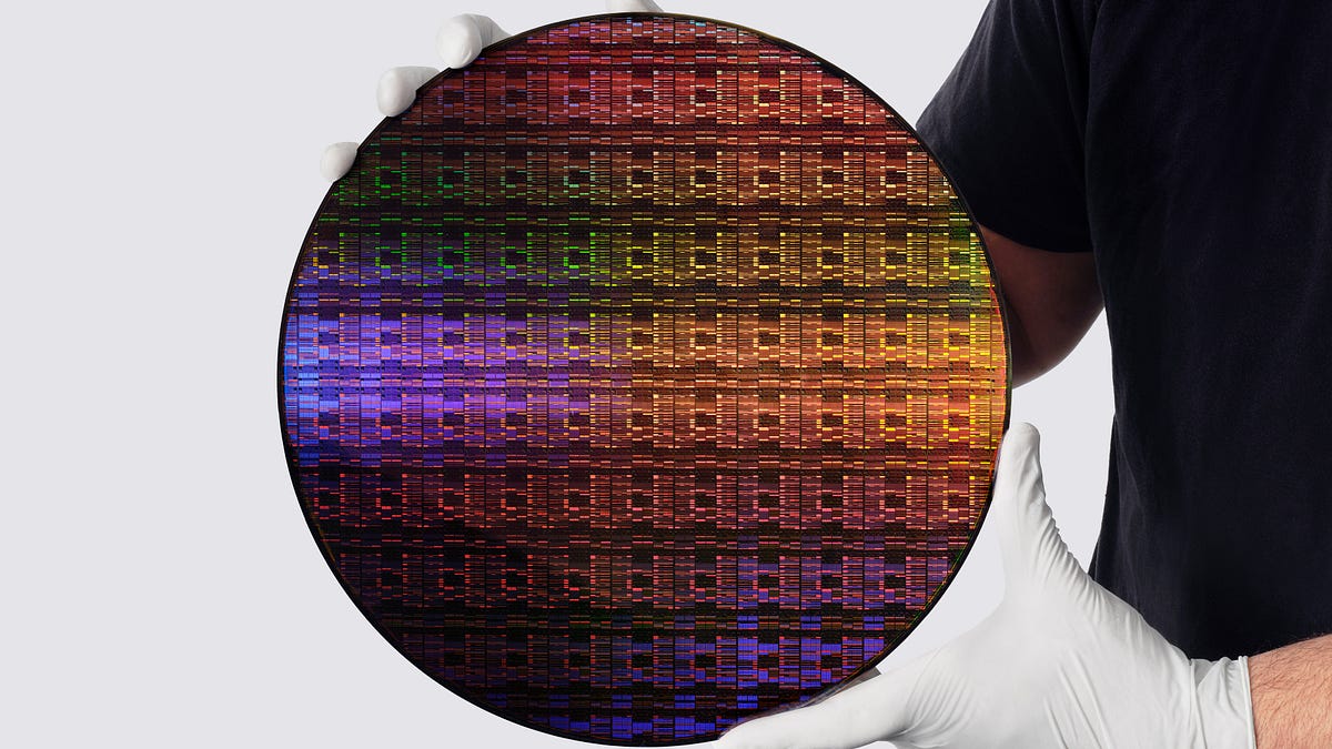
I believe IBM does most its semiconductor manufacturing research at Albany Nanotech Complex (ANTC), probably with less than 1000 researchers and technicians.

"The Albany NanoTech Complex is owned and operated by NY CREATES (New York Center for Research, Economic Advancement, Technology, Engineering and Science). NY CREATES is a state-backed, non-profit organization established by New York State to streamline the management, funding, and operations of the state's high-tech semiconductor assets."
2) tool are provided by other partners there for research, Does the state own those tools or does ASML etc.

New York State and federal grants paid for the facility, the cleanroom, and some of the expensive tools (such as EUV tools). IBM rents the space from ANTC and shares certain high cost tools (including the EUV systems, which are also owned by ANTC) with other tenants.

3) Does IBM get paid to be there or pay to use the site? does Intel or Micron or samsung use this site?

It’s complicated. But for profit driven companies (such as Micron and IBM) the costs are ultimately paid by Micron and IBM’s customers (such as Rapidus) and by taxpayers.

Here is a summary created by Google AI:

Yes, IBM pays rent and operational fees to utilize the facilities at the Albany NanoTech Complex (ANTC), but their usage of advanced tools like EUV machines is governed by a shared-cost partnership rather than simple pay-per-use renting.

Because the facility operates under a unique public-private model, IBM's financial arrangement with NY CREATES (the complex's owner) is divided into distinct categories:

1. Direct Office and Laboratory Rent

IBM must pay standard commercial rent for the physical real estate it occupies on the ANTC campus. This is approved via fixed-term leases by the NY CREATES board: [1, 2]
  • Office & Lab Space: As a primary tenant, IBM leases extensive square footage across multiple buildings (including the ZEN and NanoFab Reflection buildings).

  • Cost Structure: Lease agreements dictate specific square-footage costs, such as roughly $45 per square foot for office space and $94 per square foot for cleanroom laboratory spaces, which include operating expenses and utility pass-throughs.

  • Expansion: For instance, IBM pays roughly $930,000 annually just to lease an extra 50,000-square-foot tier of cleanrooms and engineering environments to support its scaling operations. [1, 2]

2. Tool Access: "Buy-In" Partnerships (Not Tool Rental)

IBM does not pay a conventional "hourly fee" or standard rental price to use a machine like an ASML High-NA EUV lithography tool. Instead, tool access is granted through joint-venture capital investments:
  • Consortium Funding: To gain access to the newly established High-NA EUV Center, IBM, Micron, and other tech titans entered a $10 billion joint initiative with New York State. Industry players collectively contributed $9 billion toward procuring the machinery and building out the infrastructure.

  • Shared Operating Costs: Rather than individual equipment usage bills, IBM pays an ongoing share of the facility’s broader consortium operational costs. This covers specialized engineering staff, extreme cleanroom power grids, tool calibrations, and the massive amounts of chemical consumables required to keep the machines running.

3. Joint Development Agreements (JDAs)

Because ANTC is an open-innovation ecosystem, IBM frequently offsets tool costs by signing cross-collaborative agreements with tool manufacturers on-site:
  • IBM works hand-in-hand with tool giants like Tokyo Electron (TEL), SCREEN Semiconductor, and Lam Research directly inside the Albany cleanrooms.

  • Under these agreements, the tool makers provide the hardware and technical support, while IBM provides the structural chip designs and operational expertise. The entities share both the costs of running the machinery and the patents generated from the research.

Summary

IBM pays fixed real estate rent to NY CREATES to house its hundreds of scientists on campus, but its right to use multi-million-dollar EUV machinery is secured by billion-dollar upfront capital contributions and collaborative R&D pool funding rather than a retail machine-rental fee.

Who pays IBM for IBM process research? not GF or Intel..... Do they have any partners other than Rapidus? or is it just government grants

Because IBM no longer has a fab, the majority of its new process research is funded by US taxpayers (you and me) and by Japanese taxpayers through the Rapidus project. So far, the only client for IBM’s leading edge semiconductor manufacturing technology developed at the Albany Nanotech Complex is Rapidus in Japan.

So the funny thing is that American taxpayer money is effectively helping Japan rebuild its leading edge logic semiconductor manufacturing capacity. Intel, TSMC, Samsung, and GlobalFoundries (all have US based fabs) either don’t want to use IBM’s technologies or have no need for them.
 
Last edited:
A great article from Ian Cuttress -- partial take-aways to not spoil the full article:

- "When it comes to IBM, I firmly believe they’re in the camp of saying Moore’s Law is still alive."
- There are multiple types of CFET design in the literature, and specifically IBM has built a staggered sequential CFET design
- [Compared to IBM's 2nm - 40% SRAM scaling, 50% Logic scaling, more info in article]
- IBM is getting a High-NA machine..

The article also contrasts the major chip foundries approaches to future transistor types with what IBM is doing/planning, using plenty of charts and diagrams.


"When it comes to IBM, I firmly believe they’re in the camp of saying Moore’s Law is still alive.".


IBM has labs but no fabs. Moore's Law is a problem or concept for those who are actually "manufacturing" the chips. IBM can say whatever it wants. And IBM has little skin in the game. The High NA EUV machine will be paid for by grants.
100% agreed. Though if Rapidus is successful at 2nm, I think that could also be considered a success for IBM.
 
I think hist78 has a good explanation of how IBM keeps going: IBM's customers are 1) Albany Nanotech, as a partnership; IBM provides personnel, Albany Nano the tools 2) Tool manufacturers who subsidize the tools in return for testing data, and probably a pretty open-kimono relationship 3) Materials (chemicals, photoresist, slurries, etc) suppliers who are willing to subsidize and open the kimono, in return for testing data and a process-of-record in the new process.

The patents and technology are owned by IBM, not the tool makers or materials suppliers, or Albany Nanotech. Despite considerable financial subsidies from IBM's partners. So not every organization in the industry approaches IBM with open arms. When you treat suppliers like this, they tend to hold back something from the relationship. Perhaps this is the structural reason why IBM process tends to underperform.
 
Last edited:
Back
Top