

Webinar: Enabling Next Generation Lithography Through Computational Mask and Wafer Metrology

Time: 9:00AM Central Europe | 4:00PM China | 5:00PM Japan/Korea
Featured Speakers:
- Jirka Schatz, Applications Engineer, Synopsys
- Wolfgang Demmerle, Product Manager, Synopsys
Metrology data is the foundation for lithography models which play an essential role in process development and photomask creation.
In contrast to conventional gauge-based metrology, the extraction of scanning electron microscope (SEM) image contours allows to efficiently analyze complex 2D structures and curvilinear pattern on mask and wafer.
Synopsys S-Metro provides a powerful toolbox for automated assessment of image-based SEM data, focusing on fast and robust, equipment-independent contour extraction and comprehensive analysis.
Why You Should Attend:
In this Synopsys webinar, we demonstrate how S-Metro helps lithography, mask, and OPC engineers to efficiently take advantage of SEM image contours, reducing metrology tool time and accelerating the time to obtain analysis results.
We will cover a broad range of applications, from mask characterization and defect analysis to the creation and validation of mask and wafer process models for OPC and verification.
Featured Speakers
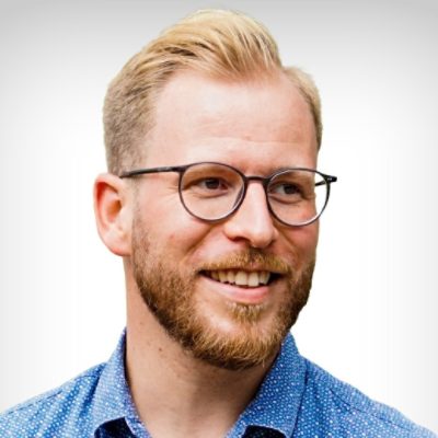
Jirka Schatz
Applications Engineer, Synopsys
Jirka is a Sr. Staff Applications Engineer in Synopsys’ Silicon Technology Group, supporting S‑Metro and S‑Litho products. He brings extensive experience in rigorous lithography simulation and model building, SEM contour metrology, process characterization, and OPC. Jirka has authored multiple publications across these disciplines. He has worked in the industry since 2009 and holds a professional degree in microtechnology for semiconductors.
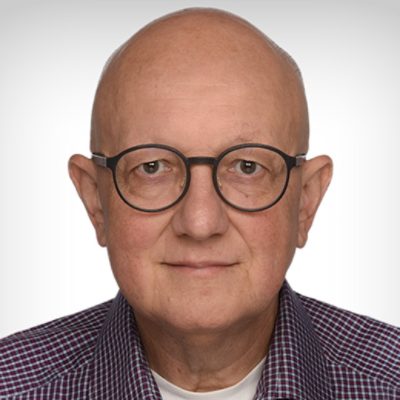
Wolfgang Demmerle
Product Manager, Synopsys
Wolfgang is a product manager for Synopsys’ computational lithography and metrology solutions, focusing on rigorous lithography simulation and scanning electron microscope (SEM) metrology data analysis. Before joining Synopsys in 2006, Wolfgang gained lithography process experience through engineering positions at Nikon and ASML. He received a doctor’s degree in Semiconductor Physics from the Technical University of Munich (Germany).


CEO Interview with Jerome Paye of TAU Systems