The year is 1999 and I decided that is time to try something else in layout. In 1989 in Israel I was part of the biggest chip in the world, the Motorola DSP9600. In 1998 in Canada I was part of the biggest Synchronous DRAM in the world, it was time to try analog/mixed signal/RF projects.
The opportunity came from PMC Sierra who already had a digital team in Ottawa and wanted to build a Mixed Signal team here. Tad Kwasniewski and Bill Bereza and myself started a new local group for Mixed Signal Design and Layout. Back to hire and train people, setup a new group, etc.
The rest of PMC was in 0.18-microns process and I needed to ensure that we have a proper setup, flow, tools, verification, etc. The success of our first local chip CRSU-10G, OC-192 was in jeopardy without proper setup in a new 0.13-micron process with a pretty aggressive project in mind for year 2000. Having a solid system in MOSAID for Electromigration thanks to Graham Allan I knew what has to be done. I shared the concept in my book original book version in 1999. The complexity of Electromigration is much bigger when you have to deal with huge buffers that drive 32 mA outputs. In this case the CML cells had source device of 3200-micron width in 0.13 microns so the metal size and number of vias arrays were crucial to be correct. Extracting information from SPICE models file I build a new 0.13 Electromigration table, yes, the layout guy 😊.
However, when I wanted to release it for use Colin Harris, advised me to get approved by the reliability department. I shared the file with Khai Nguyen, who was our PhD in reliability. After a few simulations he accepted my table and this became law for layout and design, but only for 0.13 microns. Two years later when we had major hiccup in another project, PMC decided to treat Electromigration much more seriously. Jurgen Hissen, one of mixed signal designers with a flair for programming, wrote an entire software to check it, a novelty in 2002. Peter O’Shea the new reliability PhD prepared a training course and Electromigration became a law for all Mixed Signal Design and Layout. More about this in the next book revision coming this year.
New design types bring new challenges. In MOSAID my problem was to verify big memory chips with millions of devices, in PMC the output of Mixed Signal Layout was actually small. Our blocks had up to 100k devices so using a hierarchical tool had no specific value. We were using Diva for online during development and Calibre for final GDSII. This meant that we needed for every process to qualify and maintain 2 verification tools from 2 different vendors. I invited Carey Robertson and Dan Chapman to talk to me in Vancouver. I knew that Calibre was a 2 licences software, one flat and one hierarchical, so I wanted to ask for a solution to my “IP level” verification. I explained them that if they can cut a licence that is “limited by number of devices” they can sell even more Calibre as people will replace DIVA. The calculation was simple: If the user can use a single verification deck for small blocks as well as for full chip, they can sell more licences and we (the users) can qualify/calibrate only one deck per process. In this case I even built their business case so it was a no brainer…
I had to reach Joseph Sawicki to get the ball rolling but by end of 2000 the Calibre CB (Cell & Block) with various device limitations was born, PMC Sierra ditched DIVA and the rest is history… How is this for a layout designer extracurricular activity?
I always liked competition and I knew that if only one company has a tool for my world, they will stop improving. I volunteered to work with all EDA vendors on perfecting their tools. One of my old friends from MOSAID, Jean Crepeau, now in Synopsys, got me another interesting engagement. A team from Victor, NY needed help to improve COSMOS, the Virtuoso competitor. For many quarters they drove 700 KM round trip for one day in Ottawa. They brought with them a computer disk which we hook up to a PMC desktop and we spent time reviewing features, idea, action and results from previous visit, etc. We had lot fun and the software was ready for market release but politics killed it and nobody was there to save at least the team. All this knowledge lost and Synopsys invented the new IC Designer/ Galaxy / etc… A novelty feature that was available in 2002 in COSMOS was Resistance and Capacitance as you route a signal, in this case based on a table like the Electromigration one. It knew how to calculate # of vias and metal width table based. Will talk more about this when we reach EAD software from Cadence.
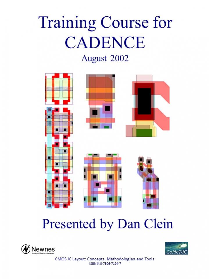
 In 2002 CADENCE decided that their verification team working on DIVA & Assura & Vampire & … can benefit from some training on flows. I worked with Gregg and updated the training material done for Mentor and worked with Beverly Higazi to organize the CADENCE visit. This time the training was actually challenging. For 5 days in the same class I had PhD in physics or software and Bachelors of Art, people with 20 years’ experience and new hires. Our material in this case was “too little” or “too much”, so the training room got very tense in the first day. I agreed with Beverly to work “overtime” and clarify some physics notions and concepts for the people who never had to deal with terms like resistance and capacitance. It was another success story and I have only good memories and a lot of pictures from this experience. We all learnt a few new things. I found again that training may be one of my future hobbies and the need for simple explanations.

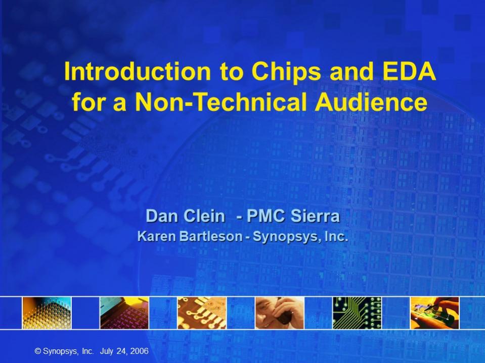
I participated in Design Automation Conference (DAC) for 20 years and followed all their announcements for tutorials, workshops, etc. A new initiative coming from Synopsys. Karen Bartleson who was at that time a Marketing Director, was presenting at DAC a 2 hours tutorial called: “Introduction to Chips and EDA for non-technical audience.” Her intention was to train people outside engineering, lawyers, financial people, etc. 10,000 feet view of the VLSI industry and the relation to EDA organizations.
I always had to battle with support organizations to explain what we are really doing in VLSI, why do I want to hire aggressive people sometimes with poor “soft skills” and how important “thinking outside the box” is for our success. Karen agreed to let me audit the training and later provided me with the original material with the condition that will be used internally and free. I added a lot of company specific information like job descriptions and a few pages from my book to make it more specific.
I used this course many times in the last 10 years to train HR, Finance, IT, purchasing, document control, etc. In one of the pilots one of the financial controllers who worked in VLSI industry for 20 years wrote me:
“Thank you for your course, now I can explain my family what the company is actually doing and what is my personal contribution to the company success.”
The course isfree but the rewards are “priceless”.
More to come so stay put…
Dan Clein, view the rest of the series…
Share this post via:


Captain America: Can Elon Musk Save America’s Chip Manufacturing Industry?