Improve productivity by shifting left LVS
In modern semiconductor design, technology nodes continue to shrink and the complexity and size of circuits increase, making layout versus schematic (LVS) verification more challenging. One of the most critical errors designers encounter during LVS runs are shorted nets. Identifying and isolating these shorts early in the process is crucial to meeting deadlines and ensuring a high-quality design. However, isolating shorts in early design cycles can be a time-consuming and resource-intensive task because the design is “dirty” with numerous shorted nets.
To tackle this challenge, designers need an LVS solution for rapid short isolation that enhances productivity by addressing shorts early in the design flow. This article explores the key difficulties designers face with short isolation, and a novel solution that integrates LVS runs with a debug environment to make the verification process faster and more efficient.
The challenge of shorted nets in LVS verification
Design size, component density, and advanced nodes like 5 nm and below all contribute to the growing complexity of SoC designs. With layouts containing billions of transistors, connectivity issues like shorted nets can proliferate. Shorts can occur between power/ground networks or signal lines and may result from misalignment, incorrect placement, or simply the close proximity of electrical connections in densely packed areas of the chip.
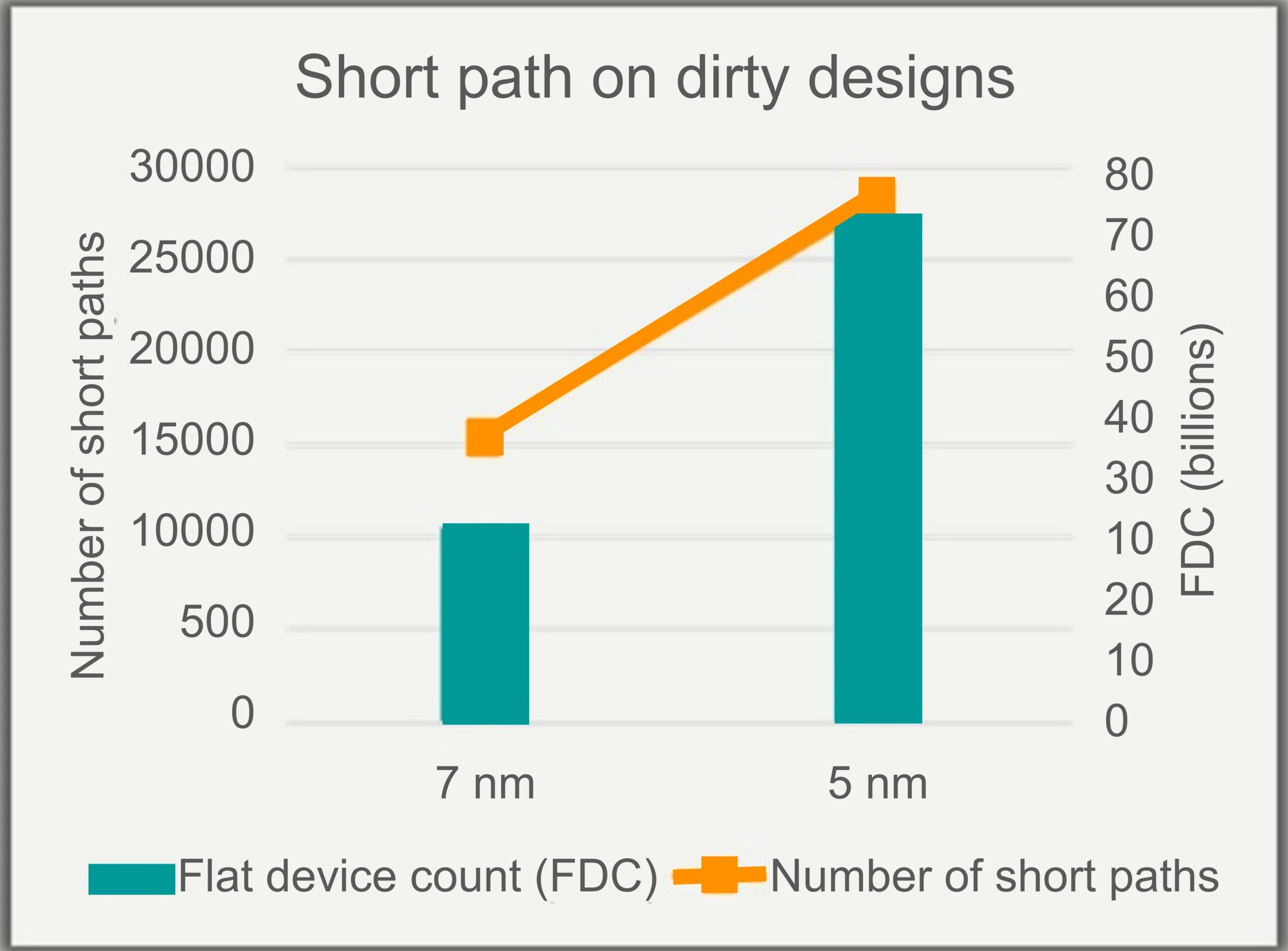
As shown in industry conference surveys, the number of shorts in “dirty” early-stage designs has skyrocketed as process nodes have shrunk, leading to an increased need for comprehensive short isolation (Figure 1). While earlier nodes like 7 nm might see a manageable number of shorts, modern 5 nm designs can produce over 15,000 short paths that need to be investigated, analyzed, and corrected. Identifying the specific short paths causing the issue is not just difficult—it’s overwhelming.

Traditional LVS verification and short debugging approaches require designers to switch between a graphical user interface (GUI) for short inspection and a command-line environment for LVS reruns, resulting in longer design cycle times and less efficient workflows. Furthermore, manually inspecting and debugging each short path is an incredibly tedious process, especially when designers need to pinpoint shorts in hierarchical designs where components and interconnects are densely packed across multiple layers.
Debugging shorts: common pitfalls
The key challenges designers face during short isolation and debugging include:
- Locating the exact short path: Each short is composed of multiple paths, and identifying the specific path responsible for the short can be time-consuming.
- Extended LVS cycle times: Running a full LVS verification after each short fix significantly lengthens the process.
- Tedious visual inspection: Manually inspecting and analyzing short paths across the entire chip layout can take several days, especially in large, complex designs.
With these challenges in mind, having an efficient short isolation solution can drastically improve the speed and accuracy of the LVS process.
A comprehensive solution for interactive short isolation
To address these challenges, Siemens EDA has developed the Calibre RVE Interactive Short Isolation (ISI) flow, which integrates short analysis directly into the Calibre RVE environment. This solution allows designers to quickly identify and debug shorts without leaving the familiar layout viewing and debugging interface.
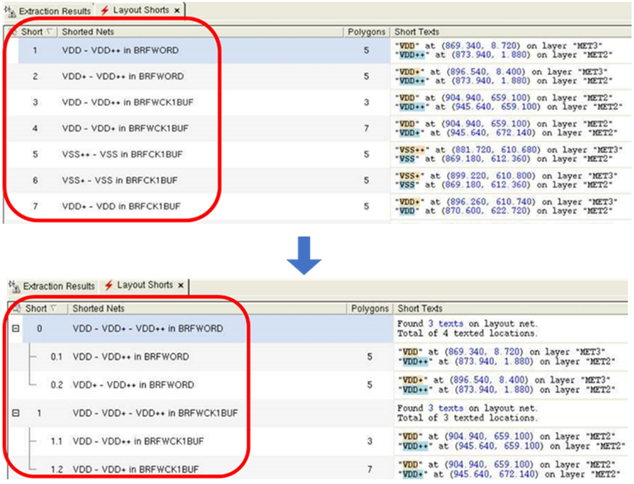
The flow lets designers visualize short paths in their design layouts after running LVS verification. With the addition of the “SI” keyword (short isolation) in the Mask SVDB Directory statement of the rule file, designers can isolate and inspect shorts in real time. The flow automatically highlights shorted segments in the layout and organizes them in an intuitive tree view, making it easier to manage and debug shorts (Figure 2).

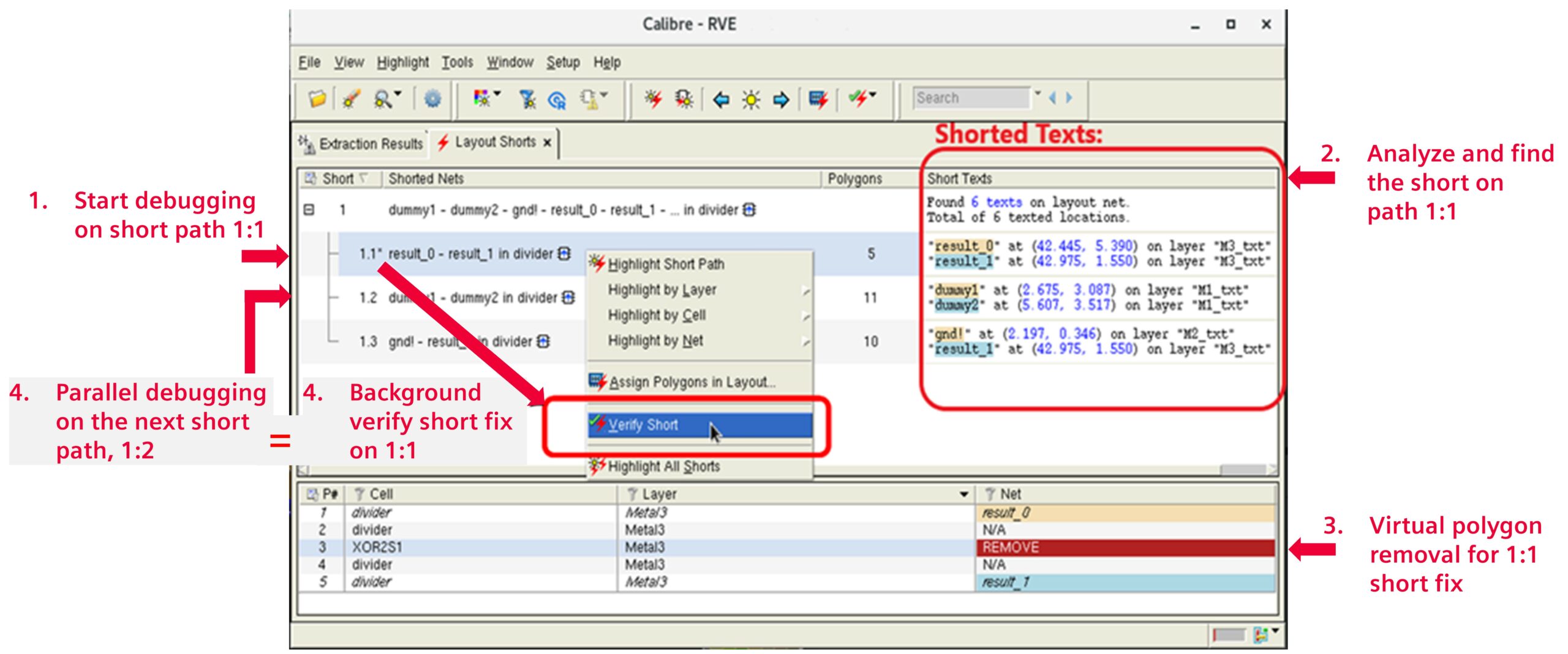
The ability to simulate short fixes without making actual changes to the design layout is a key feature. Designers can perform virtual fixes, verify them, and save the results in a separate database. This means they can debug multiple short paths simultaneously, reducing the overall LVS cycle time and minimizing disruptions to their workflow.
Benefits of short isolation in early-stage design
By running partial LVS checks targeted at specific nets, designers can quickly isolate and fix shorts on power/ground or signal nets, significantly reducing the number of shorts before running a full LVS signoff extraction.
With the integration of LVS runs into a graphical debug environment, designers no longer need to switch between different tools for verification and debugging. Instead, they can invoke LVS runs directly from the debug GUI (Figure 3). This push-button feature allows for quick, targeted LVS runs, with options for multithreading and distributed processing to further accelerate runtimes.

This short isolation flow helps designers simulate short fixes and verify them without requiring full-chip LVS runs. This targeted, parallel processing reduces overall verification time, allows for early identification of critical issues, and helps design teams stay on schedule.
Boosting designer productivity with integrated short isolation
The tight integration between Calibre tools enables a much more efficient LVS process by providing a unified toolset for short isolation, debugging, and verification. Designers can now:
- Run targeted partial LVS checks for shorts without waiting for full-chip LVS runs.
- Perform interactive short isolation and virtual fixes in the same environment.
- Automatically update results in the debug interface, eliminating the need for manual context switching.
- Leverage parallel processing and multithreading options to speed up debugging.
This seamless flow significantly reduces the time spent on short isolation and debugging, enabling designers to focus on optimizing other aspects of their design.
Conclusion: Faster SoC verification with early short isolation
As SoC designs become larger and more complex, early-stage short isolation and verification are critical to keeping projects on schedule. By allowing designers to simulate short fixes and verify them in parallel, this flow helps reduce the number of full LVS iterations required, leading to shorter design cycles and improved productivity. With the combined LVS and debug environments, design teams can tackle the most critical LVS violations early, ensuring higher-quality designs and faster time to market.
To learn more about how Calibre nmLVS Recon can streamline your verification process, download the full technical paper here: Siemens EDA Technical Paper.
Ritu Walia is a product engineer in the Calibre Design Solutions division of Siemens EDA, a part of Siemens Digital Industries Software. Her primary focus is the development of Calibre integration and interface tools and technologies.
Also Read:
Navigating Resistance Extraction for the Unconventional Shapes of Modern IC Designs
SystemVerilog Functional Coverage for Real Datatypes
Automating Reset Domain Crossing (RDC) Verification with Advanced Data Analytics
Share this post via:


