You are currently viewing SemiWiki as a guest which gives you limited access to the site. To view blog comments and experience other SemiWiki features you must be a registered member. Registration is fast, simple, and absolutely free so please,
join our community today!
By Todd Burkholder and Per Viklund, Siemens EDA
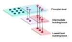
The landscape of advanced IC packaging is rapidly evolving, driven by the imperative to support innovation on increasingly complex and high-capacity products. The broad industry trend toward heterogeneous integration of diverse die and chiplets into advanced semiconductor… Read More
Todd Burkholder and Andras Vass-Varnai, Siemens EDA
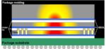
As semiconductor devices become smaller, more powerful and more densely integrated, thermal management has shifted from an afterthought to a central challenge in modern IC design. In contemporary 3D IC architectures—where multiple chiplets are stacked and closely arrayed—power… Read More