You are currently viewing SemiWiki as a guest which gives you limited access to the site. To view blog comments and experience other SemiWiki features you must be a registered member. Registration is fast, simple, and absolutely free so please,
join our community today!
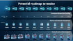
NanoIC has announced a major expansion of its process design kit portfolio with the introduction of its first A14 logic and embedded eDRAM memory PDK. This milestone reflects the company’s growing role in enabling advanced semiconductor design at cutting-edge technology nodes and addresses increasing industry demand for… Read More
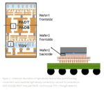
In the rapidly evolving landscape of semiconductor technology, imec’s recent breakthroughs in wafer-to-wafer hybrid bonding and backside connectivity are paving the way for CMOS 2.0, a paradigm shift in chip design. Introduced in 2024, CMOS 2.0 addresses the limitations of traditional CMOS scaling by partitioning… Read More