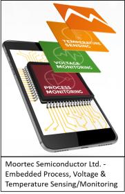
In a former life I was the GM of a business where we built specialized structures used for semiconductor process bring-up, characterization and monitoring. These monitoring structures were placed in wafer scribe-lines and were used to monitor key parameters during wafer processing. The structures provided feedback to automated… Read More
Tag: hotspots
Magic? No! It’s Computational Lithography
The industry plans to use 193nm light at the 20nm, 14nm, and 10nm nodes. Amazing, no? There is no magic wand; scientists have been hard at work developing computational lithography techniques that can pull one more rabbit out of the optical lithography hat.
Tortured metaphors aside, the goal for the post-tapeout flow is the same… Read More


