You are currently viewing SemiWiki as a guest which gives you limited access to the site. To view blog comments and experience other SemiWiki features you must be a registered member. Registration is fast, simple, and absolutely free so please,
join our community today!
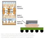
In the rapidly evolving landscape of semiconductor technology, imec’s recent breakthroughs in wafer-to-wafer hybrid bonding and backside connectivity are paving the way for CMOS 2.0, a paradigm shift in chip design. Introduced in 2024, CMOS 2.0 addresses the limitations of traditional CMOS scaling by partitioning… Read More
In the rapidly evolving semiconductor landscape, imec’s recent breakthroughs in wafer-to-wafer hybrid bonding and backside technologies are reshaping the future of compute systems. As detailed in their article, these innovations transition CMOS 2.0 from a conceptual framework to practical reality, enabling denser,… Read More
– We just finished the most happy SEMICON West in a long time
– IMEC stole the show- HBM has more impact than size dictates
– Has Samsung lost its memory mojo? Is SK the new leader?
– AI brings new tech issues with it – TSMC is still industry King
Report from SEMICON West
The crowds at Semicon West were both… Read More