You are currently viewing SemiWiki as a guest which gives you limited access to the site. To view blog comments and experience other SemiWiki features you must be a registered member. Registration is fast, simple, and absolutely free so please,
join our community today!
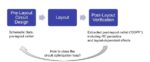
My IC design career started out with manually sizing transistors to improve performance, while minimizing layout area and power consumption. Fortunately we don’t have to do manual transistor sizing anymore, thanks to EDA tools that are quicker and more accurate than manual methods. MunEDA is an EDA vendor that has developed… Read More
Regular Semiwiki readers are aware of the rapid emergence of various (multi-die) advanced package technologies, such as: FOWLP (e.g., Amkor’s SWIFT, TSMC’s InFO); 2D die placement on a rigid substrate (e.g., TSMC’s CoWoS); and, 2.5D “stacked die” with vertical vias (e.g., any of the High Bandwidth Memory,… Read More
Digital verification engineers have developed robust, thorough metrics for evaluating design coverage. Numerous tools are available to evaluate testbenches against RTL model descriptions — e.g., confirming that simulation regressions exhaustively exercise signal toggles, RTL statement lines, individual statement… Read More