By Su Ziyun | Published October 2, 2025, 5:15 PM
According to Korean media reports, Samsung Electronics has begun the conceptual design and early development of high-bandwidth flash memory (HBF) products, preparing to join a new round of battle in the memory market.
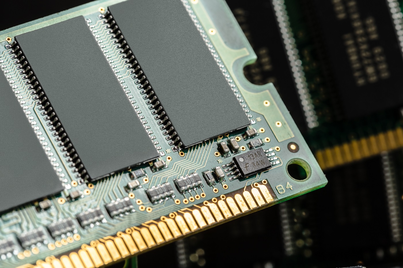
HBF's design concept is similar to HBM, both using through-silicon via (TSV) technology to connect multiple layers of stacked chips. The difference is that HBM uses DRAM as its core, while HBF utilizes NAND flash memory, which offers higher capacity and more cost-effective features.
As data centers' demand for memory capacity increases, existing NAND capacity is becoming increasingly insufficient. Furthermore, HBM is volatile memory, losing all data upon power loss. Pairing it with non-volatile NAND Flash ensures data preservation while also meeting high-speed computing requirements. Therefore, the market is expected to gradually shift towards a dual-architecture model featuring HBM + HBF to meet the dual demands of high bandwidth and large capacity for AI computing power.
SK Hynix and SanDisk were the first to initiate HBF standard development and have signed a memorandum of understanding, aiming for sample delivery in 2026 and mass production in 2027. Meanwhile, Japan's Kioxia showcased its ultra-high-speed prototype in August of this year , demonstrating its technological prowess. These moves demonstrate that HBF has become a new battleground for global memory manufacturers, actively developing their presence.
Samsung Electronics , the leader in NAND flash memory market share, has officially entered the fray , seen as a key force potentially changing the market's trajectory. According to TrendForce data, Samsung's global NAND market share rose slightly to 32.9% in the second quarter , thanks to increased demand for enterprise-class SSDs driven by AI servers. Samsung maintains its top position. If this advantage is translated into the HBF market, it will make it difficult for other companies to enter the market.
As AI models rapidly expand in size , HBM alone may be unable to fully support the massive demands of data centers. Therefore, the industry is beginning to explore the potential of HBF as a complementary solution. If successfully implemented, HBF has the potential to provide GPUs with greater data capacity while ensuring low latency and reducing unnecessary costs.
 technews.tw
According to Korean media reports, Samsung Electronics has begun the conceptual design and early development of high-bandwidth flash memory (HBF) products, preparing to join a new round of battle in the memory market.
HBF's design concept is similar to HBM, both using through-silicon via (TSV) technology to connect multiple layers of stacked chips. The difference is that HBM uses DRAM as its core, while HBF utilizes NAND flash memory, which offers higher capacity and more cost-effective features.
As data centers' demand for memory capacity increases, existing NAND capacity is becoming increasingly insufficient. Furthermore, HBM is volatile memory, losing all data upon power loss. Pairing it with non-volatile NAND Flash ensures data preservation while also meeting high-speed computing requirements. Therefore, the market is expected to gradually shift towards a dual-architecture model featuring HBM + HBF to meet the dual demands of high bandwidth and large capacity for AI computing power.
SK Hynix and SanDisk were the first to initiate HBF standard development and have signed a memorandum of understanding, aiming for sample delivery in 2026 and mass production in 2027. Meanwhile, Japan's Kioxia showcased its ultra-high-speed prototype in August of this year , demonstrating its technological prowess. These moves demonstrate that HBF has become a new battleground for global memory manufacturers, actively developing their presence.
Samsung Electronics , the leader in NAND flash memory market share, has officially entered the fray , seen as a key force potentially changing the market's trajectory. According to TrendForce data, Samsung's global NAND market share rose slightly to 32.9% in the second quarter , thanks to increased demand for enterprise-class SSDs driven by AI servers. Samsung maintains its top position. If this advantage is translated into the HBF market, it will make it difficult for other companies to enter the market.
As AI models rapidly expand in size , HBM alone may be unable to fully support the massive demands of data centers. Therefore, the industry is beginning to explore the potential of HBF as a complementary solution. If successfully implemented, HBF has the potential to provide GPUs with greater data capacity while ensuring low latency and reducing unnecessary costs.
HBF 爭奪戰開打,傳三星加入挑戰 SK 海力士與鎧俠
根據韓媒報導,三星電子已著手展開高頻寬快閃記憶體(HBF)產品的概念設計與初期開發,準備加入記憶體市場新一輪戰局。 HBF 的設計理念與 HBM 相似,皆透過矽穿孔(TSV)技術 將多層晶片堆疊連接。不同之處在於,HBM 以 DRAM 為核心,而 HBF 則採用 NAND 快閃記憶體,具備容量更大、...
technews.tw