SK Hynix presented a recent IEEE paper describing an architecture combining High-Bandwidth Memory (HBM) speed and High-Bandwidth Flash (HBF) capacity on a single interposer connecting both to a GPU to accelerate AI model and agent inference processing.
Current GPUs and the forthcoming Nvidia Rubin device have interposer-connected HBM to supply data at high speed and bandwidth to the GPU cores. However, HBM capacity limits are lengthening AI large language model (LLM) inference times as data has to be accessed from slower local SSDs. HBF is slower to access than HBM, although much faster than a local SSD, and has higher capacity. Placing it on the same interposer as HBM, as in SK Hynix’s H³ design, allows it to be used as a fast-access HBM cache, shortening large model processing time.
This is how we could conceptualize the idea:
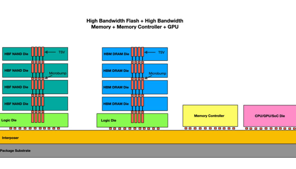
B&F diagram showing HBM, HBF, and GPU interposer-based connectivity
Future HBM generations will extend HBM capacity and bandwidth but will not arrive soon enough to address current inference latency issues, which leaves GPUs memory-bound and waiting for data.
The paper argues that H³ is well-suited to this problem in the KV cache area of inference processing. When an AI model is being used for inference, it stores the context memory sequence – component tokens and vectors – in HBM in what is called a KV (key-value) cache structure. The H³ paper states: "The latest Llama 4 [LLM] supports sequence lengths up to 10 million." This can require a 5.4 TB cache, "requiring dozens of GPUs just to store these values."
Nvidia's ICMSP software extends the KV cache to local NVMe SSDs so that they enable the processing to complete much faster than if the tokens and vectors had to be recomputed when HBM capacity runs out.
However, providing a KV cache even closer to the GPU, getting rid of the SSD PCIe bus link time, and delivering lower latency and higher bandwidth access than the local SSD is what HBF provides. The paper states: "The expected advantages of HBF are 1) up to 16x larger capacity than HBM, and 2) similar bandwidth to HBM, and the expected disadvantages are 1) slower access (ns vs. μs), 2) lower write endurance, and 3) up to 4x higher power consumption than HBM."
Because HBF has limited endurance – only supporting approximately 100,000 write cycles – it is best suited to read-intensive workloads. The H³ paper abstract says: "H³-equipped systems can process more requests at once with the same number of GPUs than HBM-only systems, making H³ suitable for gigantic read-only use cases in LLM inference, particularly those employing a shared pre-computed key-value cache."
Cache-augmented generation (CAG) is such a workload. "When the LLM receives a query, it reads the gigantic shared pre-computed KV cache, performs a computation, and then outputs a response. In other words, the shared precomputed KV cache is inherently read-only."

IEEE SK Hynix H³ paper combined HBM and HBF structure diagrams
The H³ paper diagrams show the concept. D2D is die-to-die transfer. The HBM and HBF controllers are each located on their own base die. Model weights and shared pre-computed KV caches are stored in the HBF. The generated KV caches and other data are stored in the HBM. To compensate for the longer NAND flash latency, a latency hiding buffer (LHB), which is a kind of pre-fetch buffer, is integrated into the base die of the HBM in this diagram.
The H³ design envisages a GPU having HBM stacks attached to its edges (shoreline) with both GPUs and HBM sitting on an interposer (a) in the diagram. The HBM and HBF are connected daisy-chain fashion. "Within the HBM base die, memory access is divided into two paths by address decoder and router: one accessing the HBM and the other accessing the HBF. Consequently, the GPU can directly access the HBF through the HBM base die."
"In other words, both the HBM and HBF serve as the GPU's main memory." The diagram's base global address scheme shows how "the [GPU] host uses the unified address space with divided memory regions when accessing HBM or HBF."
SK Hynix's H³ design simulation testing involved using an Nvidia Blackwell GPU (B200) with 8 x HBM3E stacks and 8 x HBF stacks. In terms of tokens per second, H³ is 1.25x higher with 1 million tokens and 6.14x higher with 10 million tokens than with HBM alone.
The results showed a 2.69x improvement in performance per watt compared to tests with a Blackwell GPU and 8 x HBM stacks but no HBF.
With testing of a KV cache with 10 million tokens, this showed that an HBM+HBF setup could process 18.8x more simultaneous queries, its batch size, than an HBM-only configuration. By using HBF, such workloads, which could include 32 GPUs and their HBM, can be processed with only two GPUs, substantially reducing electricity consumption.
Read the H³ paper for more details, particularly of the simulation testing. It costs $36 from the IEEE for non-members. Click the red PDF link on this webpage to buy a copy.
 www.blocksandfiles.com
Current GPUs and the forthcoming Nvidia Rubin device have interposer-connected HBM to supply data at high speed and bandwidth to the GPU cores. However, HBM capacity limits are lengthening AI large language model (LLM) inference times as data has to be accessed from slower local SSDs. HBF is slower to access than HBM, although much faster than a local SSD, and has higher capacity. Placing it on the same interposer as HBM, as in SK Hynix’s H³ design, allows it to be used as a fast-access HBM cache, shortening large model processing time.
This is how we could conceptualize the idea:
B&F diagram showing HBM, HBF, and GPU interposer-based connectivity
Future HBM generations will extend HBM capacity and bandwidth but will not arrive soon enough to address current inference latency issues, which leaves GPUs memory-bound and waiting for data.
The paper argues that H³ is well-suited to this problem in the KV cache area of inference processing. When an AI model is being used for inference, it stores the context memory sequence – component tokens and vectors – in HBM in what is called a KV (key-value) cache structure. The H³ paper states: "The latest Llama 4 [LLM] supports sequence lengths up to 10 million." This can require a 5.4 TB cache, "requiring dozens of GPUs just to store these values."
Nvidia's ICMSP software extends the KV cache to local NVMe SSDs so that they enable the processing to complete much faster than if the tokens and vectors had to be recomputed when HBM capacity runs out.
However, providing a KV cache even closer to the GPU, getting rid of the SSD PCIe bus link time, and delivering lower latency and higher bandwidth access than the local SSD is what HBF provides. The paper states: "The expected advantages of HBF are 1) up to 16x larger capacity than HBM, and 2) similar bandwidth to HBM, and the expected disadvantages are 1) slower access (ns vs. μs), 2) lower write endurance, and 3) up to 4x higher power consumption than HBM."
Because HBF has limited endurance – only supporting approximately 100,000 write cycles – it is best suited to read-intensive workloads. The H³ paper abstract says: "H³-equipped systems can process more requests at once with the same number of GPUs than HBM-only systems, making H³ suitable for gigantic read-only use cases in LLM inference, particularly those employing a shared pre-computed key-value cache."
Cache-augmented generation (CAG) is such a workload. "When the LLM receives a query, it reads the gigantic shared pre-computed KV cache, performs a computation, and then outputs a response. In other words, the shared precomputed KV cache is inherently read-only."
IEEE SK Hynix H³ paper combined HBM and HBF structure diagrams
The H³ paper diagrams show the concept. D2D is die-to-die transfer. The HBM and HBF controllers are each located on their own base die. Model weights and shared pre-computed KV caches are stored in the HBF. The generated KV caches and other data are stored in the HBM. To compensate for the longer NAND flash latency, a latency hiding buffer (LHB), which is a kind of pre-fetch buffer, is integrated into the base die of the HBM in this diagram.
The H³ design envisages a GPU having HBM stacks attached to its edges (shoreline) with both GPUs and HBM sitting on an interposer (a) in the diagram. The HBM and HBF are connected daisy-chain fashion. "Within the HBM base die, memory access is divided into two paths by address decoder and router: one accessing the HBM and the other accessing the HBF. Consequently, the GPU can directly access the HBF through the HBM base die."
"In other words, both the HBM and HBF serve as the GPU's main memory." The diagram's base global address scheme shows how "the [GPU] host uses the unified address space with divided memory regions when accessing HBM or HBF."
SK Hynix's H³ design simulation testing involved using an Nvidia Blackwell GPU (B200) with 8 x HBM3E stacks and 8 x HBF stacks. In terms of tokens per second, H³ is 1.25x higher with 1 million tokens and 6.14x higher with 10 million tokens than with HBM alone.
The results showed a 2.69x improvement in performance per watt compared to tests with a Blackwell GPU and 8 x HBM stacks but no HBF.
With testing of a KV cache with 10 million tokens, this showed that an HBM+HBF setup could process 18.8x more simultaneous queries, its batch size, than an HBM-only configuration. By using HBF, such workloads, which could include 32 GPUs and their HBM, can be processed with only two GPUs, substantially reducing electricity consumption.
Read the H³ paper for more details, particularly of the simulation testing. It costs $36 from the IEEE for non-members. Click the red PDF link on this webpage to buy a copy.
Bootnote
The IEEE H³ paper abstract says: "Large language model (LLM) inference requires massive memory capacity to process long sequences, posing a challenge due to the capacity limitations of high bandwidth memory (HBM). High bandwidth flash (HBF) is an emerging memory device based on NAND flash that offers HBM comparable bandwidth with much larger capacity, but suffers from disadvantages such as longer access latency, lower write endurance, and higher power consumption. This paper proposes H³ , a hybrid architecture designed to effectively utilize both HBM and HBF by leveraging their respective strengths. By storing read-only data in HBF and other data in HBM, H³ equipped systems can process more requests at once with the same number of GPUs than HBM-only systems, making H³ suitable for gigantic read-only use cases in LLM inference, particularly those employing a shared pre-computed key-value cache. Simulation results show that a GPU system with H³ achieves up to 2.69x higher throughput per power compared to a system with HBM-only. This result validates the cost-effectiveness of H³ for handling LLM inference with gigantic read-only data."
SK Hynix proposes HBM and HBF hybrid for LLM inference
SK Hynix presented a recent IEEE paper describing an architecture combining High-Bandwidth Memo ...