Date : 2026-01-22 10:04
Samsung Electronics will introduce the 'extreme ultraviolet (EUV) pellicle', a key component that will increase the productivity of advanced semiconductor processes, for the first time at the Taylor fab being built in the United States. Until now, it was unclear whether it would be introduced, but the application was virtually confirmed by ordering key equipment.
According to industry reports on the 22nd, Samsung Electronics has placed an order for EUV pellicle equipment at Taylor Fab in Texas, USA. FST will receive an order for 25 billion won worth of EUV pellicle removal and attachment equipment and inspection equipment.
EUV pellicles are ultra-thin protective components that are mounted on photomasks in the exposure process. Semiconductors embody light on a photomask with a circuit drawn in advance and embody it on a wafer. By applying EUV pellicles, it is possible to prevent fine particles and contaminants from sticking to the surface of the photomask, thereby mitigating yield degradation.
In order to use EUV pellicles in exposure equipment, special equipment for removing and attaching pellicles and inspection equipment to check the condition are required, and it was decided to bring them to the Taylor fab. The FST equipment supports not only next-generation carbon nanotube (CNT) EUV pellicles but also existing metal silicide (MeSi) EUV pellicles.
Previously, TSMC, a competitor, has been gradually introducing Japan's Mitsui Chemical's metal silicide EUV pellicles since 2019 and applying them to advanced processes.
Samsung Electronics has invested in S&Stech and FST in 2020 and 2021, respectively, to promote the localization of EUV pellicles. With the investment in related facilities this time, it is analyzed that a certain degree of performance has been secured and its introduction is imminent. This means that the durability and transmittance, which are the core performance indicators of EUV pellicles, have reached a satisfactory level.
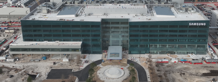
An industry official said, "Currently, the quality evaluation of EUV pellicles is underway, but it is positive that the tailor fab will be equipped with equipment on the premise of mass production application." Taylor Fab is a semiconductor manufacturing facility that Samsung Electronics is building with the goal of starting mass production of 2 nanometers (nm) in the second half of this year. Tesla's artificial intelligence (AI) chip 'AI5' is also scheduled to be mass-produced here within the year.
Samsung Electronics has more than 70 units of EUV equipment, the second largest after TSMC. As a result, it is expected that the introduction of domestically produced EUV pellicles will have a significant impact on the equipment and parts industry. The price of EUV pellicles is estimated to be more than 60 million won.
Reporter Park Jin-hyung jin@etnews.com
 www.etnews.com
Samsung Electronics will introduce the 'extreme ultraviolet (EUV) pellicle', a key component that will increase the productivity of advanced semiconductor processes, for the first time at the Taylor fab being built in the United States. Until now, it was unclear whether it would be introduced, but the application was virtually confirmed by ordering key equipment.
According to industry reports on the 22nd, Samsung Electronics has placed an order for EUV pellicle equipment at Taylor Fab in Texas, USA. FST will receive an order for 25 billion won worth of EUV pellicle removal and attachment equipment and inspection equipment.
EUV pellicles are ultra-thin protective components that are mounted on photomasks in the exposure process. Semiconductors embody light on a photomask with a circuit drawn in advance and embody it on a wafer. By applying EUV pellicles, it is possible to prevent fine particles and contaminants from sticking to the surface of the photomask, thereby mitigating yield degradation.
In order to use EUV pellicles in exposure equipment, special equipment for removing and attaching pellicles and inspection equipment to check the condition are required, and it was decided to bring them to the Taylor fab. The FST equipment supports not only next-generation carbon nanotube (CNT) EUV pellicles but also existing metal silicide (MeSi) EUV pellicles.
Previously, TSMC, a competitor, has been gradually introducing Japan's Mitsui Chemical's metal silicide EUV pellicles since 2019 and applying them to advanced processes.
Samsung Electronics has invested in S&Stech and FST in 2020 and 2021, respectively, to promote the localization of EUV pellicles. With the investment in related facilities this time, it is analyzed that a certain degree of performance has been secured and its introduction is imminent. This means that the durability and transmittance, which are the core performance indicators of EUV pellicles, have reached a satisfactory level.
An industry official said, "Currently, the quality evaluation of EUV pellicles is underway, but it is positive that the tailor fab will be equipped with equipment on the premise of mass production application." Taylor Fab is a semiconductor manufacturing facility that Samsung Electronics is building with the goal of starting mass production of 2 nanometers (nm) in the second half of this year. Tesla's artificial intelligence (AI) chip 'AI5' is also scheduled to be mass-produced here within the year.
Samsung Electronics has more than 70 units of EUV equipment, the second largest after TSMC. As a result, it is expected that the introduction of domestically produced EUV pellicles will have a significant impact on the equipment and parts industry. The price of EUV pellicles is estimated to be more than 60 million won.
Reporter Park Jin-hyung jin@etnews.com
삼성, 美 테일러에 'EUV 펠리클' 우선 도입…양산 임박
삼성전자가 첨단 반도체 공정 생산성을 높일 핵심 부품 '극자외선(EUV) 펠리클'을 미국에 구축 중인 테일러 팹에 처음 도입한다. 그동안 도입 여부가 불투명했으나 핵심 장비를 발주하며 사실상 적용을 확정 지었다. 22일 업계에 따르면 삼성전자는 미국 텍사스주 테일러 팹
www.etnews.com

