I think with EDA workflows, the relevant processes are Intel 3, 18A, 14A, and 12. My primitive understanding is that Intel 12 utilises the same machines as Intel 7.That's a new addition, seems close to Intel 16. Maybe an expected small contribution?
Intel 7 seems was in Foundry plan in earlier self-assessment (below), now about to be gone like 20A, leaving a hole.
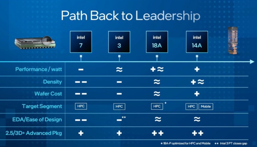
Intel Foundry Operating Model Shown with Path to Process Leadership
Intel showed its financials as Intel Foundry and Intel Products while also pointing to a potentially better futurewww.servethehome.com
View attachment 2859
Array
(
    [content] =>
    [params] => Array
        (
            [0] => /forum/threads/intel-reportedly-sticking-with-tsmc-as-part-of-new-long-term-partnership-strategy-amid-underwhelming-18a-yields.22245/page-2
        )

    [addOns] => Array
        (
            [DL6/MLTP] => 13
            [Hampel/TimeZoneDebug] => 1000070
            [SV/ChangePostDate] => 2010200
            [SemiWiki/EmailDomainReplace] => 1000010
            [SemiWiki/Newsletter] => 1000010
            [SemiWiki/WPMenu] => 1000010
            [SemiWiki/XPressExtend] => 1000010
            [ThemeHouse/XLink] => 1000970
            [ThemeHouse/XPress] => 1010570
            [XF] => 2031070
            [XFI] => 1060170
        )

    [wordpress] => /var/www/html
)
Guests have limited access.
Join our community today!
Join our community today!
You are currently viewing SemiWiki as a guest which gives you limited access to the site. To view blog comments and experience other SemiWiki features you must be a registered member. Registration is fast, simple, and absolutely free so please, join our community today!
You are using an out of date browser. It may not display this or other websites correctly.
You should upgrade or use an alternative browser.
You should upgrade or use an alternative browser.
Intel reportedly sticking with TSMC as part of new long-term partnership strategy amid underwhelming 18A yields
- Thread starter fansink
- Start date
Xebec
Well-known member
Likewise, trusting rumor sites posting random yield numbers is also probably not a good strategyFor nearly a decade, Intel’s words rarely match its actions, and ever fewer still blindly follow their lead. GL
")
Xebec
Well-known member
Didn't Nvidia have issues with delays because of TSMC packaging?. It's a lot of complexity, so I wouldn't just dismiss it. That was even on a mature node.It's strategic to blame anything other that 18a yields, such as some obscure packaging issue.
It's definitely possible 18A has real problems - it's a lot of new tech at once, but packaging issues have caused delays even at TSMC made products. If Panther lake does or doesn't launch this year then we'll know.
in the end Intel is all bark and no biteIntel is seemingly shifting its strategy of no longer outsourcing wafers to third parties to instead embracing a longer partnership with TSMC. This could be due to the unfavourable yields from Intel’s own 18A process.
It was recently reported that Intel may be pushing back its production of the next gen Panther Lake mobile processors due to unsatisfactory yields from the in-house 18A semiconductor manufacturing process. Now, according to the latest Intel earnings call, the company has announced a long-term partnership with TSMC for outsourcing wafers used for manufacturing its processors. The call, transcribed by Seeking Alpha, was between Intel’s John Pitzer and Morgan Stanley’s Joe Moore.
Intel has been struggling with bringing semiconductor manufacturing in-house as 18A, the process developed by Intel Foundry, has not presented favourable yields. TSMC, on the other hand, has a much more experienced and efficient 3nm and 2nm manufacturing process. According to the earnings call between Intel’s Corporate Vice President of Investor Relations and the MD, Semiconductor Industry Analyst at Morgan Stanley, Intel has been outsourcing about 30% of its wafers, most of it to TSMC, for a while now. However, till about a year ago, Intel wanted to reduce that number down to zero.
Now, it looks like Intel has a new strategy in place which brings about a longer partnership with TSMC. “We think it's always good to have at least some of our wafers with TSMC. They're a great supplier. It creates a good competition between them and Intel Foundry,” Pitzer reportedly added.
The earnings call and new strategy comes shortly after a known industry analyst, Ming Chi Kuo, shared that Intel’s Panther Lake mobile processors production has been pushed back due to the underwhelming performance of 18A process. This meant that the company would not be able to ship Panther Lake notebooks till 2026, missing out on 2025 Q4 sales, negatively impacting 2H25 revenue, profits, and supply chain trust.
The strategy shift may suggest that Intel has realized it is better to stick with TSMC for longer, but it is unclear how this will affect the Panther Lake processors that were supposed to be the first mobile SoCs developed on 18A.
Didn't Nvidia have issues with delays because of TSMC packaging?. It's a lot of complexity, so I wouldn't just dismiss it. That was even on a mature node.
It's definitely possible 18A has real problems - it's a lot of new tech at once, but packaging issues have caused delays even at TSMC made products. If Panther lake does or doesn't launch this year then we'll know.
From what I hear the Nvidia packaging problem was on Nvidia. It was a packaging problem yes, but Nvidia owned it. Intel packaging is an unknown outside of Intel thus far. There was talk of Intel doing packaging for TSMC customers but I have not heard anything other than Intel talking about it.
Xebec
Well-known member
@fansink - here's the "hybrid bonding" packaging tech that Intel is also debuting with 18A:
 www.intel.com
"Foveros Direct 3D" - which debuts with Clearwater Forest. (Source: https://spectrum.ieee.org/intel-18a ). It is a first time use of this technology in mass production by Intel.
Cutting-edge Process Technologies for Data Center
Intel Xeon processors, codenamed Clearwater Forest, deliver Intel 18A and advanced chiplet packaging to the data center.
www.intel.com
"Foveros Direct 3D" - which debuts with Clearwater Forest. (Source: https://spectrum.ieee.org/intel-18a ). It is a first time use of this technology in mass production by Intel.
Xebec
Well-known member
Color me a little skeptical it's 100% Nvidia's fault. It cost Nvidia significantly financially the last time they made negative press about TSMC. I would also think when using a cutting edge [node, packaging tech, etc.] - that TSMC engineers would work alongside Nvidia's engineering teams throughout the design and development processes.From what I hear the Nvidia packaging problem was on Nvidia. It was a packaging problem yes, but Nvidia owned it. Intel packaging is an unknown outside of Intel thus far. There was talk of Intel doing packaging for TSMC customers but I have not heard anything other than Intel talking about it.
Clearwater Forest has several hundreds of cores, with complex packaging of up to 12 chiplets per cpu. It is very understandable that CLF has had delay because of packaging challenges (i.e. hybrid bonding) while PTL has not.Didn't Nvidia have issues with delays because of TSMC packaging?. It's a lot of complexity, so I wouldn't just dismiss it. That was even on a mature node.
It's definitely possible 18A has real problems - it's a lot of new tech at once, but packaging issues have caused delays even at TSMC made products. If Panther lake does or doesn't launch this year then we'll know.
Fortunately, the hybrid bonding issue has been resolved by IFS.
At this point, for NVDA, seemingly what TSMC really leads IFS is its advanced packaging such as CoWoS. Though I don't quite know how far behind IFS is.Color me a little skeptical it's 100% Nvidia's fault. It cost Nvidia significantly financially the last time they made negative press about TSMC. I would also think when using a cutting edge [node, packaging tech, etc.] - that TSMC engineers would work alongside Nvidia's engineering teams throughout the design and development processes.
For mobile customers such as AAPL, IFS is behind for other reasons.
siliconbruh999
Well-known member
IIRC hybrid bonding was jointly developed with AMD I doubt anyone beside AMD or maybe Apple can use itAt this point, for NVDA, seemingly what TSMC really leads IFS is its advanced packaging such as CoWoS. Though I don't quite know how far behind IFS is.
For mobile customers such as AAPL, IFS is behind for other reasons.
Last edited:
Intel is seemingly shifting its strategy of no longer outsourcing wafers to third parties to instead embracing a longer partnership with TSMC. This could be due to the unfavourable yields from Intel’s own 18A process.
Intel is finally starting to realize how weak they have become.
Intel is finally starting to realize how weak they have become.
I think one of the objectives of UCIe is to allow mix and match/flexibility.
IanCutress
Member
Don't understand why this is news. Pat said 18 months ago that they have 30% wafers at TSMC and it will trend down to (hopefully) 20% by end of decade.
They said they are determining a target, likely between15-20%.Don't understand why this is news. Pat said 18 months ago that they have 30% wafers at TSMC and it will trend down to (hopefully) 20% by end of decade.
"""
We think it’s always good to have at least some of our wafers with TSMC. They’re a great supplier. It creates a good competition between them and Intel foundry. Not quite sure what the right sort of level set is. Is it 20?
Is it 15? We’re working through that, but we will use, I think, external foundry suppliers longer kind of under this new strategy. On the Intel foundry side, I think you’re right. We’re on a mission to stand up a world class Intel foundry. I think the key point that the board wanted to stress, and I think Dave is clearly on board with this is that we’ve put a lot of our owners’ capital into that strategy over the last several years with not great financial returns today.
And I think incremental returns on incremental capital is going to be a key metric that we look at as we drive that strategy forward.
"""
Xebec
Well-known member
I think the "pundits" are trying to determine if Pats 'retirement' means there is going to be a reversal on Pats strategy to increase in sourcing.Don't understand why this is news. Pat said 18 months ago that they have 30% wafers at TSMC and it will trend down to (hopefully) 20% by end of decade.
We are in full misinformation news mode with Intel but at the same time Intel has been untrustworthy with regards to hitting it's intended dates and targets. (For a long time). (i personally hope 18A delivers on time to build some good will there though.)
MKWVentures
Moderator
All companies are doing hybrid bonding development. The question is what the cost and yields are and who ramps itIIRC hybrid bonding was jointly developed with AMD I doubt anyone beside AMD or maybe Apple can use it
siliconbruh999
Well-known member
Yes iirc Sony is the market leader in Hybrid bonding TSMC does it and Intel will soon release products based on it(assuming the delay was actually fixed)All companies are doing hybrid bonding development. The question is what the cost and yields are and who ramps it
A design company can't develop it solely anyway we will be left with the few manufacturer we have.
All companies are doing hybrid bonding development. The question is what the cost and yields are and who ramps it
Phone SoC makers are certainly not into it. They will remain volume-cost oriented.
But maybe they will pay for advanced fanout packaging.
The prime majority will remain epoxy BGA packaged for as long as something will not beat it on price.