Array
(
    [content] => 
    [params] => Array
        (
            [0] => /forum/threads/intel-foundry-is-way-behind-tsmc-but-the-goal-is-2-by-2030.24411/page-2
        )

    [addOns] => Array
        (
            [DL6/MLTP] => 13
            [Hampel/TimeZoneDebug] => 1000070
            [SV/ChangePostDate] => 2010200
            [SemiWiki/Newsletter] => 1000010
            [SemiWiki/WPMenu] => 1000010
            [SemiWiki/XPressExtend] => 1000010
            [ThemeHouse/XLink] => 1000970
            [ThemeHouse/XPress] => 1010570
            [XF] => 2030871
            [XFI] => 1060170
        )

    [wordpress] => /var/www/html
)

Intel Foundry is way behind TSMC, but the goal is #2 by 2030

Not sure I agree with the logic here. Intel's biggest need right now is to fill the fabs. Choosing not to even try to serve a large portion of the potential market doesn't seem like a winning prospect to me. Yes the upfront expense is high, but the cost of underutilized fab space is astronomical. Just like interest, the cost of unused fab space never rests, it just keeps sucking up money.

Intel's plan is for these new nodes to run for over a decade plus. That is a lot of time to recover the upfront investment. I think being too concerned about a short term up front cost is short sighted and will cost Intel more in the long run.

I also don't think Intel wants to paint themselves out of the picture to manufacture the designs that their new ASIC design business will potentially generate. With BSPD being primarily aimed at HPC applications it seems to me front side power will be more desirable for many ASIC applications. Including the option in the foundry offerings gives these ASIC customers an easy on-ramp to work with Intel foundry.
But it's not just about cost, the amount of extra resource -- meaning, engineers! -- needed to support both BSPD and FSPD processes is huge because so many things are different. For starters the layouts are completely different so all IP (both internally and externally sourced) has to be rebuilt from scratch, and it's not just a few layout tweaks it's a major rethink -- plus the extraction is different, thermal properties are very different, libraries (standard cell and SRAM) have to be redone from scratch, tool costs double, customer support effort doubles. You also have to duplicate all the process qualification/reliability analysis because the processes are physically fundamentally different, and this alone is a massive effort and takes a lot of time and wafers to do.

Intel are already likely to be stretched in all these areas just to support BSPD because traditionally they only had to support internal design teams (so crappy documentation is "OK"), much more effort/resource is needed to properly support external customers -- been there in the past, got the T-shirt. Suggesting that they could easily do all this again for FSPD is not credible, they'd end up with terrible support for both processes instead of barely adequate support for one -- TSMC have being doing all this for years on multiple processes, but that doesn't mean Intel can do the same...

It doesn't matter how much Intel might *want* do support both, the question is whether they *can* support both -- and I don't think they can, at least not today.

There's also the question of why they would realistically want to do this, because all the things that FSPD customers are looking for -- fast TTM, strong IP ecosystem, low cost, high yield, high density, quick TAT -- are the things that TSMC is *very* good at (which is why everyone uses them) and Intel is historically bad at (and still not competitive today). Fighting an opponent on a battleground where they're strong and you're weak is never going to end well... :-(

People who don't understand the huge differences between the two processes are grossly underestimating the cost and difficulty of supporting both, see post from @MKWVentures above... ;-)
agree on the non-trivial effort supporting both options. As for the adequate resource, it comes down to whether intel really seriously consider to be in the foundry business, with aspiration to challenge tsmc. Intel ONLY need to support a hands of process nodes, while tsmc has full spectrum. And yes older nodes do not need as much support, but the scope of offering and support needed are obvious a lot more than what Intel current has.

Bottom line, if one wants to play in foundry business, one has to be prepared to make the necessary investment.
Like boy scouts, being prepared is one thing, but whether you actually have the resources is another thing entirely. No amount of *wanting* to do something is suddenly going to make a large number of experienced engineers appear out of nowhere, which is what would be needed for Intel to support both BSPD and FSPD. Plus they would have needed to have started this development at least a couple of years ago to have an N2 competitor in time, and I don't think even Intel have a time machine... ;-)

And it comes down to the big question -- even if Intel can compete with TSMC on the BSPD playing field for HPC where performance/speed is all-important (which they have a good chance of doing) and things like die cost and IP availability matter little to a few big customers -- which is essentially a similar market to their historical IDM CPU one where they were very successful -- can they compete in the FSPD foundry market where cost/density/yield/TTM/IP ecosystem are more important than balls-out speed/performance at all costs, and where they've been historically unsuccessful?

If Intel top management are being honest with themselves, I'm pretty sure the answer is "no" -- unless they can recruit Dr.Who and use the Tardis to go back and change their development history... ;-)
 
But it's not just about cost, the amount of extra resource -- meaning, engineers! -- needed to support both BSPD and FSPD processes is huge because so many things are different. For starters the layouts are completely different so all IP (both internally and externally sourced) has to be rebuilt from scratch, and it's not just a few layout tweaks it's a major rethink -- plus the extraction is different, thermal properties are very different, libraries (standard cell and SRAM) have to be redone from scratch, tool costs double, customer support effort doubles. You also have to duplicate all the process qualification/reliability analysis because the processes are physically fundamentally different, and this alone is a massive effort and takes a lot of time and wafers to do.

Intel are already likely to be stretched in all these areas just to support BSPD because traditionally they only had to support internal design teams (so crappy documentation is "OK"), much more effort/resource is needed to properly support external customers -- been there in the past, got the T-shirt. Suggesting that they could easily do all this again for FSPD is not credible, they'd end up with terrible support for both processes instead of barely adequate support for one -- TSMC have being doing all this for years on multiple processes, but that doesn't mean Intel can do the same...

It doesn't matter how much Intel might *want* do support both, the question is whether they *can* support both -- and I don't think they can, at least not today.

There's also the question of why they would realistically want to do this, because all the things that FSPD customers are looking for -- fast TTM, strong IP ecosystem, low cost, high yield, high density, quick TAT -- are the things that TSMC is *very* good at (which is why everyone uses them) and Intel is historically bad at (and still not competitive today). Fighting an opponent on a battleground where they're strong and you're weak is never going to end well... :-(

People who don't understand the huge differences between the two processes are grossly underestimating the cost and difficulty of supporting both, see post from @MKWVentures above... ;-)

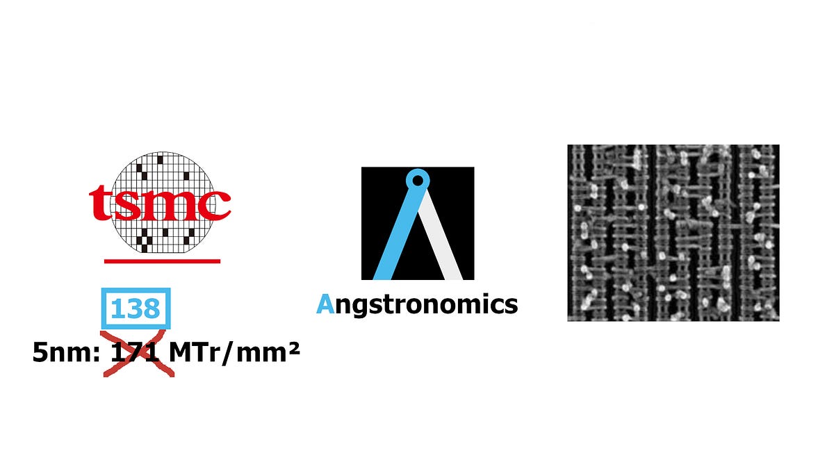
People always talk about and compare the PPA (Power, Performance, and Area) in the semiconductor industry. In reality, it should be PPAC, wit the C represents the cost. Without managing the cost, customers won't come because they won't make enough profit to justify why they need to buy your products or services.

For example, Intel has one of the largest R&D budgets in the semiconductor industry, yet its R&D returns have been miserable for years.

1769623194720.png
 
Like boy scouts, being prepared is one thing, but whether you actually have the resources is another thing entirely. No amount of *wanting* to do something is suddenly going to make a large number of experienced engineers appear out of nowhere, which is what would be needed for Intel to support both BSPD and FSPD. Plus they would have needed to have started this development at least a couple of years ago to have an N2 competitor in time, and I don't think even Intel have a time machine... ;-)

And it comes down to the big question -- even if Intel can compete with TSMC on the BSPD playing field for HPC where performance/speed is all-important (which they have a good chance of doing) and things like die cost and IP availability matter little to a few big customers -- which is essentially a similar market to their historical IDM CPU one where they were very successful -- can they compete in the FSPD foundry market where cost/density/yield/TTM/IP ecosystem are more important than balls-out speed/performance at all costs, and where they've been historically unsuccessful?

If Intel top management are being honest with themselves, I'm pretty sure the answer is "no" -- unless they can recruit Dr.Who and use the Tardis to go back and change their development history... ;-)
given the direction of the new management, which is much more certainly of ROI before any investment, they are playing a very LONG game.
 
Like boy scouts, being prepared is one thing, but whether you actually have the resources is another thing entirely. No amount of *wanting* to do something is suddenly going to make a large number of experienced engineers appear out of nowhere, which is what would be needed for Intel to support both BSPD and FSPD. Plus they would have needed to have started this development at least a couple of years ago to have an N2 competitor in time, and I don't think even Intel have a time machine... ;-)

And it comes down to the big question -- even if Intel can compete with TSMC on the BSPD playing field for HPC where performance/speed is all-important (which they have a good chance of doing) and things like die cost and IP availability matter little to a few big customers -- which is essentially a similar market to their historical IDM CPU one where they were very successful -- can they compete in the FSPD foundry market where cost/density/yield/TTM/IP ecosystem are more important than balls-out speed/performance at all costs, and where they've been historically unsuccessful?

If Intel top management are being honest with themselves, I'm pretty sure the answer is "no" -- unless they can recruit Dr.Who and use the Tardis to go back and change their development history... ;-)

By and large, each Scout is competing against himself or herself, not against other Scouts. Once a Scout completes the required milestones, merit badges and community service, he or she advances to the next rank, such as Eagle Scout.

Intel, however, operates in a completely different environment. Intel and every other semiconductor company are competing directly against one another. Simply being prepared is not enough.

Thank you for bringing up the “Boy Scouts” analogy. It suddenly made me realize that Intel has been in “Scout mode” for many years. It has achieved a lot internally and showcased many accomplishments at conferences and trade shows, but that isn’t enough in the highly competitive semiconductor industry.
 
agree on the non-trivial effort supporting both options. As for the adequate resource, it comes down to whether intel really seriously consider to be in the foundry business, with aspiration to challenge tsmc. Intel ONLY need to support a hands of process nodes, while tsmc has full spectrum. And yes older nodes do not need as much support, but the scope of offering and support needed are obvious a lot more than what Intel current has.

Bottom line, if one wants to play in foundry business, one has to be prepared to make the necessary investment.

The other problem is Samsung selling leading edge wafers so cheaply. Being as good as TSMC and as cheap as Samsung is a rock and a hard place.
 
Maybe Intel can help Elon build his Terafabs he mentioned today. Maybe Ohio ??

"You know, I mentioned this at the shareholder meeting, but even when we look at the best case output of all of our key suppliers, and I’d say even they’re beyond suppliers, they’re like strategic partners, like Samsung, TSMC, and Micron, and we say, like: "What’s the most you could possibly make?" Then it’s not enough. So I think in order to remove the constraint, the probable constraint in three or four years, we are gonna have to build a Tesla Terafab, a very big fab that includes logic, memory, and packaging, domestically. And that’s actually also gonna be very important to ensure that we are protected against any geopolitical risks.

I think people may be underweighting some of the geopolitical risks that are gonna be a major factor in a few years. So, now, you know, a lot of people are like, "That’s crazy. Fabs are really hard." I’m like: "Yes, I know fabs are really hard. I don’t think they’re easy." But we do a lot of hard things. You know, we didn’t used to have car factories, that we didn’t use to have battery cell factories or lithium refineries or, you know, Megapack factories or, you know, all these other things. We figured it out. So I think we-- if we don’t do the Tesla Terafab, we’re gonna be limited by supplier output of chips. And I think maybe memory is an even bigger limiter than AI logic. So you know, for example, we have chip supply deals with TSMC in Arizona and Samsung in Texas, but currently there are no advanced memory fabs at scale in the United States. There are zero, literally zero.

Hopefully, you know, Micron will have something going in a few years, because they’re all headquartered in Idaho, you know, where they make a lot of potato chips, but they need to make computer chips, too. So, anyway, we’re working with our strategic partners on the chip front, memory and logic, but I think we’ve got to also try our hand at building a large-scale fab that integrates logic, memory, and packaging. And if we don’t do that, we’re just gonna be fundamentally limited by supply chain, especially if there’s some geo- in a worst-case geopolitical situation, it would be quite a severe situation. So I think -- quite frankly, it’d be crazy not to try the Terafab."

 
Plus they would have needed to have started this development at least a couple of years ago to have an N2 competitor in time, and I don't think even Intel have a time machine... ;-)
If you look back at my initial post you will see that I specifically called out FSPD on 14A. I never claimed it was on their N2 competitor which is 18A. That is a product that has just rolled out the PDK 0.5. Intel expects customer orders to ship in 2028. If they follow TSMC's path FSPD will show up around a year later like 16A is planned to. So they have roughly 3 years to do the development. No time machine required.

Regarding the complexity, I do work in a fab and frequently interact with integration. So while I don't claim to be an expert, I am not totally ignorant of process flows and the type of changes switching from BSPD to FSPD would entail.
 
Samsung Foundry is behind TSMC, trying to catch/mimic TSMC as much as possible but yield is still low

Intel 5N4Y = Intel 7, Intel 4/3, Intel 20A/18A in 2021-2025, big changes like FinFET->GAA, Backside Power, ..
Samsung 3N3Y = SF3 in 2024, SF2 in 2025, SF2P in 2026, same GAA & small changes like reducing M0 Pitch, ..
According to news reporters in Korea, Samsung is expecting/guiding external customers to adopt SF2P

1769663267912.png
1769662522451.png
 
If you look back at my initial post you will see that I specifically called out FSPD on 14A. I never claimed it was on their N2 competitor which is 18A. That is a product that has just rolled out the PDK 0.5. Intel expects customer orders to ship in 2028. If they follow TSMC's path FSPD will show up around a year later like 16A is planned to. So they have roughly 3 years to do the development. No time machine required.

Regarding the complexity, I do work in a fab and frequently interact with integration. So while I don't claim to be an expert, I am not totally ignorant of process flows and the type of changes switching from BSPD to FSPD would entail.
I don't know where you get 18A being a competitor to N2 from -- 18A competes with N3, 14A competes with A16 which is the BSPD version of N2, and following on a year or so behind it. TSMC did N2 FSPD first and then A16 BSPD, Intel have done 14A BSPD first (and only?) with no plan for FSPD as far as I can see, so they're not "following TSMCs path".

And given the market for FSPD, Intel coming along at least a year later than TSMC and with higher wafer cost and lower gate density would mean nobody would choose them, unless desperate or for strategic reasons -- and FSPD 14A would already have to be on the roadmaps and in development, with customers already designing into it. Intel have missed the boat for FSPD with this node... :-(

The raw process change is a big issue for sure, but there are others too -- apart from the time/effort for process reliability qualification (FSPD and BSPD are physically very different, so are stresses and interactions with packaging), but even once you have the process built and qualified the elephant in the room is IP and libraries... ;-)

Generating in-house ones is a big effort in itself -- again, there are big differences in the two, not just layout but the way that power meshes and self-heating behave is very different (no common design, different tool flow). And the even bigger elephant in the room is externally-developed IP and libraries which a huge proportion of foundry customers either develop themselves (the big guys) or buy in, and here the TSMC ecosystem is absolutely enormous, Intel are nowhere in comparison -- and IP developers are going to be reluctant to invest in developing IP for Intel with few (or no...) guaranteed customers, their ROI would be terrible, much better to invest in more TSMC development where they know there will be customers.

That's the reality of bleeding-edge chip design today, the raw process is of little use to many customers without the IP and library support, and this is where TSMC excels -- pretty much any building block you need will be available (and usually qualified on silicon) from *somebody*, and there are *lots* of somebodies... :-)
 
Last edited:
I don't know where you get 18A being a competitor to N2 from -- 18A competes with N3, 14A competes with A16 which is the BSPD version of N2, and following on a year or so behind it. TSMC did N2 FSPD first and then A16 BSPD, Intel have done 14A BSPD first (and only?) with no plan for FSPD as far as I can see, so they're not "following TSMCs path".
isn't the difference between A16 and A14 in single digits even from TSMC's slides
 
isn't the difference between A16 and A14 in single digits even from TSMC's slides
What difference do you mean -- cost, power, speed, density? Rate of improvement in all these per mode is getting slower and slower... :-(

It looks like A14 is really a shrunk N2 with FSPD targeted at mobile, not a shrunk A16 with BSPD (SPR) targeted at HPC...

1769690742841.png


Key Improvements from A16 to A14
  • Performance & Efficiency: A14 is designed to deliver roughly 16% higher performance or 27% lower power consumption than N2, building upon the ~8-10% speed boost A16 provides over N2P.
  • Density Gains: A14 provides a >20% density gain over N2, representing a full-node scaling successor compared to the ~1.1x improvement of A16.
  • Technology Advancement: While A16 focuses on integrating Super Power Rail (SPR) for high-performance computing (HPC), A14 utilizes 2nd Generation GAA transistors for improved mobile and AI performance.
  • Design Flexibility: A14 features enhanced NanoFlex Pro for superior cell optimization, following the NanoFlex concept introduced earlier.
 
I don't know where you get 18A being a competitor to N2 from -- 18A competes with N3, 14A competes with A16 which is the BSPD version of N2, and following on a year or so behind it. TSMC did N2 FSPD first and then A16 BSPD, Intel have done 14A BSPD first (and only?) with no plan for FSPD as far as I can see, so they're not "following TSMCs path".

And given the market for FSPD, Intel coming along at least a year later than TSMC and with higher wafer cost and lower gate density would mean nobody would choose them, unless desperate or for strategic reasons -- and FSPD 14A would already have to be on the roadmaps and in development, with customers already designing into it. Intel have missed the boat for FSPD with this node... :-(
I guess we will have to agree to disagree. Time will tell us who has the better crystal ball. :)
 
Back
Top