You are currently viewing SemiWiki as a guest which gives you limited access to the site. To view blog comments and experience other SemiWiki features you must be a registered member. Registration is fast, simple, and absolutely free so please, join our community today!
It is his fault! He has some external people who could and can tell him what is required and what the gap and problems are. Sadly given how things are going and what we hear and see the listening and change isn’t happening fast enough
On this supply chain part i find it funny if some incident happens everyone will be left blank face like in covid
Anyways for the D0 part is 0.4 good i found a slide from tsmc N7/N5 while searching online considering 18A was going to be HVM ready in 2H24
I think this other slide from the Aug 2020 TSMC tech symposium is more helpful.
Assuming Panther lake mobile SOCs launch in September like prior gen ICL/TGL/LNL SOCs, then 18A would currently be -4Q from MP (sept in this graph). Assuming the -4Q DD trend from TSMC follows the same slope it was on in Q3, then 18A measures up similarly to N5 at that point, a bit worse than N7 and alot better than 10FF.
tsmc's N2 HVM is projected for Q4 2025. Assuming that both tsmc and Intel experience similar yield trend improvements, the D0 trend for tsmc's N2 and Intel's 18A could align on a similar timeline.
While Intel claims its 18A process will be "manufacture-ready" in the second half of 2024, ahead of tsmc's N2 HVM, in reality, Intel 18A doesn’t seem to have a timeline advantage.
So, is the only advantage of adopting Intel 18A the reduced geographic risk?
Pather Lake is a mobile part. I think Nova Lake is 2026 product. D0 trend might improve by then? Because they are tile-based. I guess the yield should be better?
Pather Lake is a mobile part. I think Nova Lake is 2026 product. D0 trend might improve by then? Because they are tile-based. I guess the yield should be better?
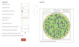
Should we multiply them to get the yield? I was thinking in terms of usable area of a wafer. It is above 60%. By matching the quantities of each tile, should the final yield also be above 60%?
You are not wrong, but I would be shocked if in one year from now the DD was still 0.4. The real question mark is what is the DD slope going to look like over the next year? It's all well and good if DD is similar to N5 at a similar time, but if the slope looks more like N7's slope than N5's we are talking like 0.18DD (64% for RPL using the same website) instead of 0.12DD (74% for RPL).
Why would you assume that multiple different partition dies are all 18A? Intel has used the statement that Pantherlake starts shifting the die area back to intel, but intel doesn't indicate they are going back to a more "normal" external foundry usage until that 2027-ish timeframe where we will likely be talking about PNL-next-next and 14A. Also 18A isn't intel's only process technology either.
Should we multiply them to get the yield? I was thinking in terms of usable area of a wafer. It is above 60%. By matching the quantities of each tile, should the final yield also be above 60%?
You're right, I was thinking about it just afterwards. I think we should just consider the separate tile yields as if they were the chip die yields.
Ideally 562,848 of each tile would just use up 451, 492, or 1056 wafers for the platform, graphics, compute cases. But due to the compute lower yield, it is now only 362,208 of each tile. So it would be 64.4%.
Why would you assume that multiple different partition dies are all 18A? Intel has used the statement that Pantherlake starts shifting the die area back to intel, but intel doesn't indicate they are going back to a more "normal" external foundry usage until that 2027-ish timeframe where we will likely be talking about PNL-next-next and 14A. Also 18A isn't intel's only process technology either.
Since Panther Lake is used for touting Intel 18A success, I had made this assumption. If it were just the compute tile, I would have expected them to be specific about that, as they were for Meteor Lake.
This part is funny.
The reality is that when Intel asks, "Are you interested in Intel's IFS, which has less geographic risk?" everyone says yes. But when they ask, "Are you going to place orders with IFS?" no one says yes.
Why would you assume that multiple different partition dies are all 18A? Intel has used the statement that Pantherlake starts shifting the die area back to intel, but intel doesn't indicate they are going back to a more "normal" external foundry usage until that 2027-ish timeframe where we will likely be talking about PNL-next-next and 14A. Also 18A isn't intel's only process technology either.
Correct PTL-H is 18A chiplet with 4P+8E+4LPE with NPU and memory controller and display logic GPU is N3E and N6 IO tile in the diagram Die 4 is 18A and Die 5 is N3 GPU
PTL-U Is 4P+4LPE with NPU/display logic and memory controller Intel 3 GPU tile and N6 IO a cheaper lunar lake from Intel Lunar lake
The source for the info
Should we multiply them to get the yield? I was thinking in terms of usable area of a wafer. It is above 60%. By matching the quantities of each tile, should the final yield also be above 60%?
Yield for die/tile is usually a fab yield indicator related only to fab and a combination of Fab line yield loss, WAC and Functional Test. Good tiles are assembled in the tile concept would be CoWoS and that yield is generally very high for mature, I can guess for the latest lCoWoS they aren’t nearly in the high 90s but better not be 60% as that would be atrociously expensive as you are throwing away multiple very expensive die at the last step, but it ain’t high 90s% as in the mature simple OSAT process