Array
(
    [content] => 
    [params] => Array
        (
            [0] => /forum/threads/imec-roadmap-to-2a-on-techtechpotato.23071/
        )

    [addOns] => Array
        (
            [DL6/MLTP] => 13
            [Hampel/TimeZoneDebug] => 1000070
            [SV/ChangePostDate] => 2010200
            [SemiWiki/Newsletter] => 1000010
            [SemiWiki/WPMenu] => 1000010
            [SemiWiki/XPressExtend] => 1000010
            [ThemeHouse/XLink] => 1000970
            [ThemeHouse/XPress] => 1010570
            [XF] => 2021770
            [XFI] => 1050270
        )

    [wordpress] => /var/www/html
)

IMEC Roadmap to 2A on TechTechPotato

benb

Well-known member

Summary
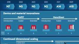
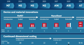
-On the left: Starting from Finfet, next is "Nanosheet"

1750519745695.png

-Lithography: From 0.33NA EUV to 0.55NA EUV starting at the second Nanosheet generation ("Scaled")
-Metal pitch: In 2025, we're at 22nm in the first generation Nanosheet. This is down from 23nm at the last Finfet node, N3. The next scaling step will take us to 21nm.
1750520163118.png

-Metal pitch, backside: The pitch is relaxed considerably on the backside wiring. Initially 160-65nm, then in the second Nanosheet generation, 115-45nm.
-Ian Cutressdescribes the last Nanosheet generation as "Forksheet". That takes us to 18nm metal pitch with A10 designation.
1750520679368.png

-This brings us to the 2031 timeframe with a new transistor: CFET ("Complementary Fet"). This stacks the GAA NMOS and PMOS transistors on top of each other, doubling density. The designation is A7.
-Ian describes the brick wall CFETs need to climb. Up to CFET, the high temperature processing used to form the transistor is done once. At CFET, it will need to be done twice. This is not a lithography challenge. It's a temperature-resistant materials challenge. And as we've found with batteries, it can be slow progress when it comes to materials. 2031 is not far off, and breakthroughs are needed.

1750521653692.png

-Assuming everything goes well with CFETs, we then move to 2DFET. This is a CFET with a single layer of a material like (Ian suggests) aluminum disulfide, tungsten ditelluride, or tungsten diselenide, a family of materials that naturally form monolayers. They grow at high temperatures which is a red brick. Junction resistance is a red brick. How to dope 2D materials is a red brick.
-Another big advance will be needed to get there: 0.75NA EUV.
1750521988954.png
 

Attachments

  • 1750519653082.png
    1750519653082.png
    476.3 KB · Views: 38
  • 1750520101604.png
    1750520101604.png
    480.6 KB · Views: 45
Full sized image for you :)

View attachment 3309
I feel like I left out my thoughts describing all the new things (CFETs, 2DFETs, 0.75NA EUV, and Back-side power). Those are 4 big, big innovations coming in the next 10ish years. Back-side power arrives very soon (2025-2026). This is not a slowing down or settling down of a mature industry, but rather a rejuvenation of innovation now that we’re over the (rather large) EUV hump.

The innovation costs will have to be incorporated in wafer prices though. So wafer costs are going to increase. One worry is if the roadmap raises costs too much for the market to bear.

Another worry is a China shock. What if China enters the roadmap at the leading edge and drives wafer prices down to the point TSMC, Intel and Samsung cannot continue investing in new nodes? Clearly that is China’s goal, and playbook.
 
Back
Top