Arthur Hanson
Well-known member
Is this tech an important breakthrough or just a small step? What impacts could this technology have and is anyone else working in this direction? Thanks
Abstract
Two-dimensional (2D) materials have extended the device scalability1,2,3 of silicon (Si) technology and enabled fundamental innovations in device mechanisms4,5,6. Both industry7,8,9 and academia10,11,12,13, particularly in the field of integrated circuits, are pursuing integration breakthroughs to demonstrate the superiority of 2D electronics at the system level. Despite considerable integration progress on either 2D material integration11,12,13 or 2D-CMOS hybrid integration14, a system that can migrate the advantages of the device to the application is still lacking.
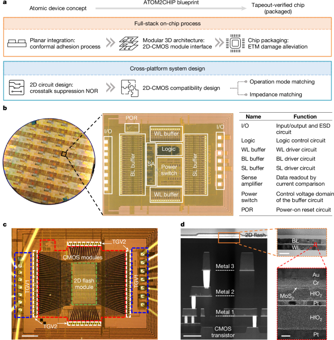
Here we report a full-featured 2D NOR flash memory chip realized by an atomic device to chip (ATOM2CHIP) technology, which combines a superior 2D electronic device as a memory core and a powerful CMOS platform to support complex instruction control. The ATOM2CHIP blueprint includes a full-stack on-chip process and a cross-platform system design, providing a complete framework to bridge the gap from emerging device concept to an applicable chip.
The full-stack on-chip process is a specially designed flow that incorporates planar integration, three-dimensional (3D) architecture and chip packaging, contributing to a high yield of 94.34% based on a full-chip test. The cross-platform system design handles both the 2D circuit design and the 2D-CMOS modules compatibility verification design, contributing to a highly complex, instruction-driven, full-featured chip with 8-bit commands and 32-bit parallelism. These results demonstrate an efficient system integration strategy that showcases the advantages of the 2D electronic system.
 www.nature.com
Abstract
Two-dimensional (2D) materials have extended the device scalability1,2,3 of silicon (Si) technology and enabled fundamental innovations in device mechanisms4,5,6. Both industry7,8,9 and academia10,11,12,13, particularly in the field of integrated circuits, are pursuing integration breakthroughs to demonstrate the superiority of 2D electronics at the system level. Despite considerable integration progress on either 2D material integration11,12,13 or 2D-CMOS hybrid integration14, a system that can migrate the advantages of the device to the application is still lacking.
Here we report a full-featured 2D NOR flash memory chip realized by an atomic device to chip (ATOM2CHIP) technology, which combines a superior 2D electronic device as a memory core and a powerful CMOS platform to support complex instruction control. The ATOM2CHIP blueprint includes a full-stack on-chip process and a cross-platform system design, providing a complete framework to bridge the gap from emerging device concept to an applicable chip.
The full-stack on-chip process is a specially designed flow that incorporates planar integration, three-dimensional (3D) architecture and chip packaging, contributing to a high yield of 94.34% based on a full-chip test. The cross-platform system design handles both the 2D circuit design and the 2D-CMOS modules compatibility verification design, contributing to a highly complex, instruction-driven, full-featured chip with 8-bit commands and 32-bit parallelism. These results demonstrate an efficient system integration strategy that showcases the advantages of the 2D electronic system.
A full-featured 2D flash chip enabled by system integration - Nature
A full-featured 2D NOR flash memory chip realized by an atomic device to chip technology combines a superior 2D electronic device as a memory core and a powerful CMOS platform to support complex instruction control.
www.nature.com