Array
(
    [content] => 
    [params] => Array
        (
            [0] => /forum/index.php?threads/will-we-ever-see-stmicro-or-gf-offer-7nm-class-chips.18171/page-2
        )

    [addOns] => Array
        (
            [DL6/MLTP] => 13
            [Hampel/TimeZoneDebug] => 1000070
            [SV/ChangePostDate] => 2010200
            [SemiWiki/Newsletter] => 1000010
            [SemiWiki/WPMenu] => 1000010
            [SemiWiki/XPressExtend] => 1000010
            [ThemeHouse/XLink] => 1000970
            [ThemeHouse/XPress] => 1010570
            [XF] => 2021370
            [XFI] => 1050270
        )

    [wordpress] => /var/www/html
)

Will we ever see STMicro or GF offer 7nm-class chips?

The Samsung/IBM collaboration is 20+ years in the making so it has had many incarnations. True, the Common Platform collaboration was a spectacular failure. IBM and GF also collaborated on a 7nm process that never made it into production and resulted in GF's pivot away from leading edge process technologies.
The last clear benefit IBM got from the CP + their own tricks was the embedded DRAM up to their last chips at GF.

There was a huge architectural change when they went to Samsung where they invested in a quite unusual large L2 per CPU which was shared coherently, even between all chips in a server, salvaging some of the performance characteristics of their prior chips. If they had not been able to keep a similar profile it would have risked pushing customers to finally migrate to other systems. For both POWER and Zxx machines any such break with backwards compat would have been unacceptable.

It was likely a bitter pill to swallow and the largest direct consequence of GF concluding that 7nm could never work, stranding IBM without a custom process that may have included an eDRAM solution. Or maybe they did not even have an eDRAM solution if the 7nm process had gone to production. Only the insiders know what happened. All we can do is read the evidence in the architectural upheaval of the Samsung generation of IBM super-CPUs. That was a big lift.

The remaining university collaboration for IBM is probably a balance based on reputation (convincing the legacy customers than IBM continues to invest in their needs) and licensing revenues. As IMEC shows, a good R&D org can be profitable, although IBM/SUNY is not nearly as collegial (hosting so much of the industry to second personnel and sponsor specific research) as IMEC. Perhaps that should be their future.
 
They still can't figure out how to make an even half-competent GPU, and have to license technology. I don't really get them, at all. Even mediocrity would be a welcome step up for them. And now they're going to compete against not just TSMC, and Intel. They better step up their game, and by that I don't mean press releases.
Their design house is not their fab division. But it is interesting to look at both Samsung and Intel as cautionary examples of what can go wrong if there is not a clean separation, and clear focus on what they need to do to be best, is the way to go.

The whole business structure is different. Different capital intensity, quite different depreciation of assets, offset market cycles, needs on both sides for diversity of process and of multiple customer input, different kind of staffing and specialities, different physical locations, etc. Only historical accident explains why a design house and a fab would be in the same company.
You can also look at Intel and say how powerful a company can be if it not only had control over designs, but also the fab. They've been extremely successful with this combination, far more successful than TSMC or AMD, or NVIDIA, when you look at it historically.

And it's why Intel is wiping the floor with AMD in market share for client computing; they don't have to pay to have someone else make their chips. It's also a good part of why they have the best single-threaded performance.

There are downsides, but let's keep it in perspective. Their fabs screwed up, big time, and their designs had security problems over the same time period. So, both parts had issues, and they had a down time because of it. That doesn't mean that having a design and fab isn't a good idea, it just means it's not a great idea to screw up for too long in such a competitive industry.

Would their fabs have survived their colossal screwups without being part of the same company as their designs? Probably, but they'd be in WAY worse shape than they are now.

I still think it's a good idea, a really good one. Historically, it's played out really well. Even now, it's not so bad that Intel 7 is doing pretty well, and Intel 4 and 3 are around the corner. I think the worst is over, and Intel, both parts, are very much intact, and undamaged. I'm not sure that would have been true if they were two separate companies.
 
What's wrong with solidifying on 14nm for devices on the edge (IoT)? It's a nice alternative to TSMC 16nm, which has far less leakage then 28nm, much more efficient than 28nm, provides more routing layers, and is a US alternative. Why do customers need to go with quadruple patterning? Perhaps GF didn't go with 7nm because they are practical.

What I don't know are the GF14 yields. We second source on GF14 because of paranoia, but never taped it out. If their 14nm yields are good, I would consider GF to be a success. Does anybody have experience with silicon on that process?
 
Last edited:
You can also look at Intel and say how powerful a company can be if it not only had control over designs, but also the fab. They've been extremely successful with this combination, far more successful than TSMC or AMD, or NVIDIA, when you look at it historically.

And it's why Intel is wiping the floor with AMD in market share for client computing; they don't have to pay to have someone else make their chips. It's also a good part of why they have the best single-threaded performance.

There are downsides, but let's keep it in perspective. Their fabs screwed up, big time, and their designs had security problems over the same time period. So, both parts had issues, and they had a down time because of it. That doesn't mean that having a design and fab isn't a good idea, it just means it's not a great idea to screw up for too long in such a competitive industry.

Would their fabs have survived their colossal screwups without being part of the same company as their designs? Probably, but they'd be in WAY worse shape than they are now.

I still think it's a good idea, a really good one. Historically, it's played out really well. Even now, it's not so bad that Intel 7 is doing pretty well, and Intel 4 and 3 are around the corner. I think the worst is over, and Intel, both parts, are very much intact, and undamaged. I'm not sure that would have been true if they were two separate companies.

"And it's why Intel is wiping the floor with AMD in market share for client computing; they don't have to pay to have someone else make their chips. It's also a good part of why they have the best single-threaded performance.".

In this market share competition against AMD, Intel is also wiping out its own profits.
 
Unless there is a huge update on packaging technology, I don´t see ST pushing towards 7nm technology.

Their strategic focus is on automotive, consumer and industrial markets. Since these markets have special requirements on the package types, they would not benefit significantly from smaller nodes. It does not make sense cost wise to use 7nm die if you would still have to pack it in an LQFP package.
Their 18nm automotive process might be a different story, as it could include more complexity for automotive computing systems. Yet I think this will address different markets than computing applications, even within automotive.
 
It does not make sense cost wise to use 7nm die if you would still have to pack it in an LQFP package.
How does the package limit the process? Interesting.
Their 18nm automotive process might be a different story, as it could include more complexity for automotive computing systems.
When it comes to the growth in automotive, from entertainment to nav to self driving, it seems more related to server chips than classic auto. Highly complex logic, lots of memory, not much analog. N7 and below look to have advantages which should motivate new packaging, not the opposite.

Sure there is also a lot of interesting analog around the EV drive train, and probably the controllers for that are mostly classic auto. Not huge logic, very reliable, harsh environment rated. But to say 7n and below has no place seems unlikely. It is clearly a growth opportunity.
 
How does the package limit the process? Interesting.

Not necessarily for the process technology itself, but it is a limitation for the typical ST customer base. Typically, automotive and industrial customers try to avoid BGA style packages whereever possible and instead prefer LQFP/QFN packages.
The "pads" (please forgive/correct me if that's not the correct terminology) for the wire bonding in these type of packages require a lot of size compared to the actual die size. This means you would need to artificially increase the size of your die. This makes no sense cost wise.

Unless someone is able to fix this issue, moving to smaller nodes would significantly increase the cost, while not adding a whole lot of value for their current customer base.
 
the wire bonding in these type of packages require a lot of size compared to the actual die size. This means you would need to artificially increase the size of your die. This makes no sense cost wise.
That makes sense. Is there a problem with the BGA? inadequate temperature range?
 
Main arguments I have heard so far are complex PCB design and end-of-line quality control. Why pick up the extra cost for few extra layers in your PCB and x-ray inspection (instead of AOI) if it´s not necessary?

Also, I am aware of some concerns in regards to use of BGA and QFN package in harsh environments, especially in areas where vibration is to be considered. LQFP packages are considered safer, since the physical soldering connection is bigger and thus has less risk of failing.
 
The "pads" (please forgive/correct me if that's not the correct terminology) for the wire bonding in these type of packages require a lot of size compared to the actual die size. This means you would need to artificially increase the size of your die. This makes no sense cost wise.
Bingo!
 
GF of 2018 was pretty close to delivering 7nm, they even had the SRAM bitcells qualified. But then Mubadala, being wholly inexperienced and nearsighted and impatient, brought in McKinsey to kill it on the doorstep and start stripping copper from the walls. Now in 2023 GF is a running joke and I'm amazed any company would do a joint investment with them given how they bailed on IBM. The one thing the CHIPS Act got right is not giving GF a dime.
 
So you think that quadruple patterning is worth it? You think that Shumer isn't going to fund the foundry in his backyard?
 
GF of 2018 was pretty close to delivering 7nm, they even had the SRAM bitcells qualified. But then Mubadala, being wholly inexperienced and nearsighted and impatient, brought in McKinsey to kill it on the doorstep and start stripping copper from the walls. Now in 2023 GF is a running joke and I'm amazed any company would do a joint investment with them given how they bailed on IBM. The one thing the CHIPS Act got right is not giving GF a dime.
They needed billions of dollars of extra investment to build a total of 15k WSPM. No matter the technological capabilities of the tech it could not have been cost competitive at volumes that low (doubly so since it was the last to ramp and would be further behind the cost and yield learning curves). As much as GF dropping out sucked, we need to be honest with ourselves. GF had over a decade to develop functioning foundry or heck even functioning nodes (and no I don't count nodes from chartered, or that they licensed). They failed at every turn, and their only 7LPP customer was IBM as AMD was committed to N7 years before 7LPP's plug got pulled. As much as I might want to, I can't exactly blame the oil money for getting tired of that money sink.
 
GF of 2018 was pretty close to delivering 7nm, they even had the SRAM bitcells qualified. But then Mubadala, being wholly inexperienced and nearsighted and impatient, brought in McKinsey to kill it on the doorstep and start stripping copper from the walls. Now in 2023 GF is a running joke and I'm amazed any company would do a joint investment with them given how they bailed on IBM. The one thing the CHIPS Act got right is not giving GF a dime.

From what I remember GF was working with IBM on 7nm. GF even bought EUV machines. Unfortunately it was DOA so GF tried to do a TSMC "like" 7nm but had no customers so the EUV machines were sold off.

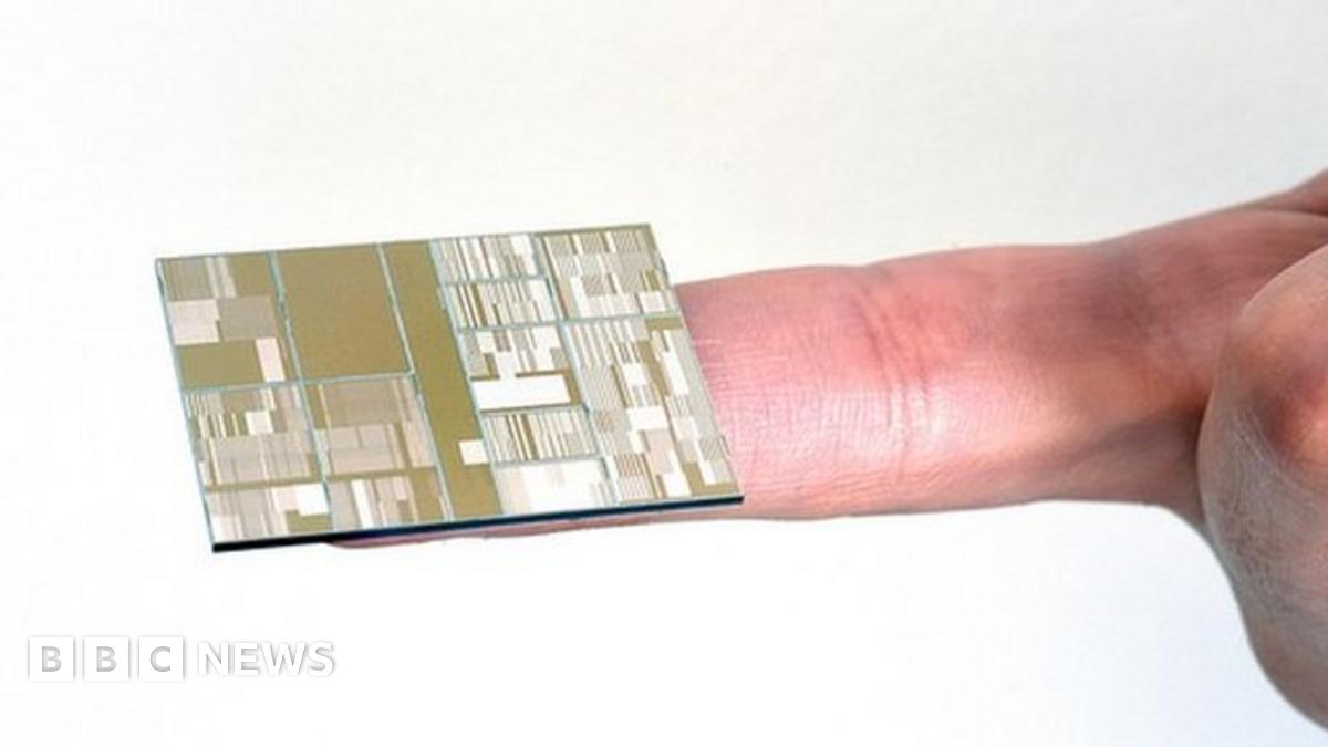
July 10, 2014 - IBM has announced that it's investing $3 billion into two R&D programs that will hopefully make it the authority on 7-nanometer-and-beyond chip technologies.

July 9, 2015 - IBM is announcing the first successful test chips at 7nm today, with multiple new innovations. The new processors will use EUV for manufacturing and SiGe-based transistors.


Samsung does make the IBM CPU chips but it is Samsung 7nm not IBM 7nm.
  • Dec 20, 2018 - IBM Expands Strategic Partnership with Samsung to Include 7nm Chip Manufacturing
  • March 23, 2021 - Intel revealed a new research partnership with IBM
IBM brings to this partnership decades of 'hard tech' semiconductor innovations that have shaped the industry, from the invention of one-transistor DRAM, to chemically amplified resists, to copper interconnects, to silicon germanium chips, to debuting the world's first 7 nanometer and 5 nanometer node test chips, to IBM’s continued innovation in the industry’s first advanced “nanosheet” device structure and electronics packaging technologies.

 
GF of 2018 was pretty close to delivering 7nm, they even had the SRAM bitcells qualified. But then Mubadala, being wholly inexperienced and nearsighted and impatient, brought in McKinsey to kill it on the doorstep and start stripping copper from the walls. Now in 2023 GF is a running joke and I'm amazed any company would do a joint investment with them given how they bailed on IBM. The one thing the CHIPS Act got right is not giving GF a dime.
Consultants for the win!!!
 
Back
Top